1. General introduction to deposition of thin films and laser interaction with materials
This general introduction will discuss the relevance of laser ablation within the general field of thin film deposition. The field of thin film deposition is characterised by a myriad of different deposition techniques, all with their specific merits and disadvantages. Most of the techniques are developed for optimal deposition of one specific material. It is far beyond the scope of this chapter to discuss the details of these various techniques, and, since most of these techniques are a variant of a more general procedure, only a few general deposition techniques will be discussed.
The film deposition techniques will be discussed in the framework of the fundamental aspects of film growth, which will be described in some detail. The important fundamental parameters for film deposition will be addressed, and the different deposition techniques will be compared. The practicalities and the (possible) use in industry of each of the techniques will be discussed also.
In addition, a few examples of other applications of laser interaction with solid materials will be presented, namely the field of surface photochemistry, Matrix Assisted Laser Desorption and Ionisation (MALDI), the use of lasers in manufacturing of photonic components and in space technology. This list is of course not exclusive, since the whole field of laser interaction with materials is still developing, but gives a representative overview of a few of the trends in the field.
At the end of this chapter the scope of this thesis will be discussed and a general overview of the contents will be given.
1.1. Description of different deposition methods
1.1.1. Description of Pulsed Laser Deposition
The pulsed laser deposition (PLD) process is both conceptually and experimentally relatively simple. A laser beam is focused onto a target material placed in a high vacuum chamber or a low pressure of background gas. The mere photon density on the target surface causes the ejection of neutral and ionised material via thermal and / or photochemical ejection mechanisms. The ejected material from a target arising after laser irradiation is called an ablation plume; it can consist of a plasma, a gas and a particulate component. The flux of material then impinges on a substrate, on which deposition takes place. The basics of the experimental technique are given in Figure 1.1.
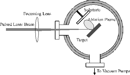
Figure 1.1: Schematic of a basic PLD system.
1.1.2. Deposition Techniques
Different deposition techniques that are used in technology are given in Table 1.1, with the acronym used to describe the technique. As discussed the introduction of this chapter, this list is far from complete, but it gives an overview of the more important competing techniques for thin film deposition.
|
Technique |
Acronym |
|
Thermal Evaporation |
TE |
|
(Accelerated) Molecular Beam Epitaxy |
(A)MBE |
|
Cathodic Arc |
CA |
|
Laser Assisted/ Metal Organic/ Plasma Enhanced/ Chemical Vapour Deposition |
LA/ MO/ PE/ CVD |
|
Sputtering (RF, Magnetron, ion beam) |
S |
|
Ion Beam Deposition |
IBD |
|
Pulsed Laser Deposition |
PLD |
Table 1.1: Different deposition techniques
TE is the easiest deposition technique, namely evaporative deposition of a target material either thermally, or by means of electron beam heating. MBE uses continuous molecular beams generated via Knudsen sources. If the beam is partially ionised by electron impact and accelerated towards the target via an electric field the process is defined as AMBE. CA uses a high current cathode/anode set-up to create a plasma from a conducting solid target, which is used as deposition flux. The deposition flux in CVD is derived from the reaction of two or more gases above a heated substrate; heating is generally necessary to sustain the reaction. Metals can be deposited by using metal-organic compounds as input gases (MOCVD) and the chemical reaction can be enhanced by sustaining a plasma above the substrate (PECVD) or by energy input via a laser beam (LACVD). Sputter deposition is performed by extracting ions (usually Ar+) from a plasma at keV energies and arranging for them to strike a target consisting of the material to be deposited. The energetic Ar+ ions produce a continuous flux of sputtered atoms that deposit on a nearby substrate. IBD distinguishes itself from the other plasma deposition techniques because the plasma is generated remotely from the substrate; the ions are extracted by ion optics and accelerated towards the substrate.
1.1.3. Film Growth
Film growth and quality are dependent on a few fundamental parameters, namely the substrate temperature, the kinetic energy of the deposition flux and the deposition rate.[1] Effects from background gas can also be included as a fundamental parameter. The importance of these parameters will be discussed, and the different techniques will be compared.
1.1.3.1. Substrate temperature
The temperature of the substrate is a highly important process parameter influencing the film morphology. In the initial stages of the film growth the flux deposited on the substrate might re-evaporate from the surface, nucleate into a cluster, be consumed by existing clusters or be trapped on a surface defect site. All these processes are dependent upon the mobility of the deposited atoms on the surface, and they each have their characteristic activation energies. Such surface rearrangements are possible at higher temperatures, while at low temperature they are inhibited.
Three modes of initial growth can be distinguished. These are shown in Figure 1.2.[2] Island (Volmer-Weber) growth results in the formation of isolated islands on the surface. This occurs when the cohesive energy of the atoms within the film is greater than the cohesive energy between the film and atoms on the surface. Layer-by-Layer (Frank - van der Merwe) growth involves a deposition of one monolayer at the time and results in a very smooth epitaxial film. It occurs when the cohesive energy between the film and the surface atoms is greater than the cohesive energy of the film atoms. The cohesive energy will decrease monotonically as each film layer is added. Mixed growth involves growth of islands after the first monolayer has formed succesfully. This occurs when the monotonic decrease in binding energy is energetically over-ridden by other factors such as strain due to lattice mismatch, with the result that island formation becomes more favourable.
The substrate temperature can have a profound influence on the film growth mechanism. For example, film growth via TE of metals has been modelled via Molecular Dynamics simulations at two different temperatures, 0 K and 0.4 Tm (where Tm is the melting temperature of the metallic film). [3],[4] Growth at 0 K is characterised as Volmer-Weber growth, while film growth at higher temperatures follows the Frank – van der Merwe growth model.
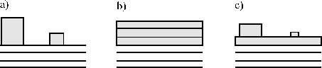
Figure 1.2: Different growth modes in thin film deposition, (a) Volmer-Weber growth, (b) Frank – van der Merwe growth and (c) mixed growth.
The substrate temperature can also have a profound influence on the film thickening.[5] The closer the temperature of the substrate to the melting temperature of the film, the more film relaxation channels are energetically accessible. At low temperatures (< 0.2 Tm), film growth proceeds via an athermal process, enabling metastable structures to grow. At higher temperatures (0.3 Tm < T < 0.5 Tm) grain boundaries within the film become mobile and surface diffusion and recrystallisation occurs. At the lower limit of this region the grain boundaries of just one preferred orientation may become mobile, giving preferential growth surfaces. At higher temperatures, surface and bulk diffusion and recrystallisation occur, yielding larger crystallites.
Clearly the microstructural morphology of the film is highly dependent on the growth temperature; indeed the temperature can be used as a process parameter to induce different structures. Metastable structures are grown preferentially at lower substrate temperatures, while the growth of crystalline materials will require higher (> 0.3 Tm) substrate temperatures to induce reconstruction and surface relaxation.
1.1.3.2. Energy of the deposition flux
Early film growth techniques employed deposition fluxes at thermal gas temperatures (> 0.1 eV). Growing films from species impinging at higher kinetic energies generally improves the film quality; this appears to have been first recognised by Mattox.[6] The effects of high kinetic energy ion bombardment of the substrate include ballistic collisions, ion mixing and thermally stimulated exchange mixing. These effects produce similar effects to raising the substrate temperature and govern film properties like film stress and crystal structure. An important manifestation of the similarity of the effects of temperature and incident kinetic energy is that high quality films can sometimes be deposited at lower substrate temperatures by using a high kinetic energy deposition flux.
The effects of a high kinetic energy deposition flux have been investigated via molecular dynamics simulations of Ag deposition on Ag at 300 K, as a function of incident particle kinetic energy.[7] The calculation showed that the film grows in islands at low kinetic energies (< 10 eV) but that layer-by-layer growth dominates at higher kinetic energies. Ion mixing was also noticeable at higher kinetic energies (> 10 eV); some of the substrate atoms are located in the film and vice versa. This effect scales with impact energy and is associated with vibrational relaxation of the interface.
The above mechanism is still distinctly different from ion mixing during high-energy ion bombardment in which the ballistic collisions induce direct displacements of substrate atoms. The extent of displacements within the substrate is governed by the kinetic energy of the incident flux via the displacement energy. For example, the displacement energy for a bulk silicon atom is ~ 22 eV. Assuming that the surface displacement energy is half of this amount (11 eV) sets a window for the ‘ideal’ deposition conditions since, within this window, surface modification considered beneficial for film growth is allowed, while bulk displacement and ion mixing are minimised. Such purely ballistic collision effects are also dependent on the substrate atom mass, and the mass of the incoming atoms, since the energy transfer during collision is dependent on the mass difference between the species involved in the collision. A detailed study of the influence of the different parameters has been reported by Brice et al.[8]
A second mechanism, in which high incident kinetic energies are important but where energy plays a contrary role to temperature, is during the growth of metastable films. The mechanism describing such film growth is the sub-plantation model,[9] which finds extensive use in discussions of the growth of Diamond Like Carbon (DLC) films. Films with the highest sp3 fraction are characteristically grown in a deposition flux kinetic energy window of 100 to 200 eV.[10] The DLC network grown under these conditions is compacted by these high-energy collisions. A deposition flux at lower energy induces to less compaction, while a deposition flux at higher energy gives rise to sputtering. In contrast, increased temperature would be expected to induce thermodynamically favoured growth of the stable structure, i.e. graphite. Thus DLC films with high sp3 content are grown preferentially at room temperature and with deposition flux kinetic energies of 100-200 eV. A consequence of this high kinetic energy is a large degree of ion mixing during deposition of these films; if grown on Si, a SiC interface exits between the film and the substrate.
1.1.3.3. Deposition Rate, vacuum quality and background gas
The rate at which material impinges on the surface (henceforth 'the deposition rate') is highly dependent on the material that is to be deposited and has to be considered on a case by case basis. Nevertheless, there are some general ground rules to consider. Too high a deposition rate will cause film deterioration because of the reduced opportunity for film relaxation. Too small a deposition rate, on the other hand, will result in unacceptably long deposition runs. The deposition rate is also correlated with the quality of the available vacuum since high deposition rates tend to put fewer demands on the vacuum quality. The lower the deposition rate, the more chance the film will incorporate unwanted gaseous impurities (common impurities include H2O, CO2, H2 and N2).
When depositing from multicomponent targets, the intentional introduction of background gas can enhance the film quality or can even enable the production of the multicomponent film (oxides or nitrides) from a monocomponent target and the appropriate reactive background gas (e.g. oxygen or nitrogen). Two additional effects can arise as a result of introducing background gas, namely, chemical reactions and / or non-reactive thermalising collisions between the energetic flux and the background gas.
Using high kinetic energy deposition fluxes in a background gas can induce gas phase reactions, which might aid in the deposition. Numerous examples can be given from the field of laser ablation, e.g. ablation of graphite in a nitrogen atmosphere under standard conditions gives rise to CN species,[11] which are easily observed from their violet emission in the ablation plasma, and lead to production of C:N films with a nitrogen content that is related to the background pressure of nitrogen. A second example is the deposition via ablation of PbZrTiO3.[12] Pb atoms in the plume can be oxidised by a background pressure of oxygen. The ablated Pb atoms thus deposit as PbO, which has a higher vapour pressure than Pb, and is retained more efficiently within the film.
Introduction of a background gas is not universally advantageous to all deposition techniques. As we have seen, the kinetic energy of highly energetic and directed fluxes can be usefully controlled by introduction of (reactive or non-reactive) background gas. On the other hand if the deposition flux does not have high kinetic energy and directionality it will be scattered by background gas collisions. In such cases the deposited film thickness drops precipitously as either the source-substrate distance or the pressure is increased.
1.1.4. Comparison of the different techniques for the different fundamental film growth parameters
Table 1.2 gives an overview of the requirements and performance of the different deposition techniques assessed against various different fundamental criteria.
|
Technique |
Energy Range (eV) |
Vacuum Requirement |
Multi-Element Control |
Background Gas |
|
TE |
0.1 |
HV |
Difficult |
No |
|
(A)MBE |
0.1/0.1-100 |
UHV |
Moderate |
No |
|
CA |
0.1-1000 |
HV |
Moderate |
Yes |
|
CVD |
0.1/0.1-500 |
HV |
Moderate |
Yes |
|
S |
1-1000 |
HV |
Easy |
No |
|
IBD |
50-1000 |
UHV |
Difficult |
No |
|
PLD |
1-1000 |
HV |
Easy |
Yes |
Table 1.2: Different deposition criteria
The fundamental criterion of temperature control is omitted from the list since substrate temperature control can be easily included in the set-up for each technique. The kinetic energy range in most of the techniques is quite versatile, with the exception of TE, which only gives thermalised fluxes. (A)MBE and IBD require ultra high vacuum because of the small film deposition rate obtained in these techniques, which make them very sensitive to contaminants.
Multi-element control refers to the ease with which deposition rates can be accurately controlled when two or more species are deposited simultaneously. This criterion is most important for deposition of electronical components, because of their sensitivity to the precise stoichiometry. Only PLD and S can be described as 'easy' when it comes to producing a given stoichiometry, since these techniques use erosion of a target material to produce the deposition flux. In all other methods the deposition flux is produced from separate sources, each carrying one of the components of the film, which imposes much higher demands on the control system to produce a given film stoichiometry.
The introduction of background gas allows the opportunity to control further the stoichiometry. PLD has a significant advantage to other techniques since it shows high versatility with regard over this criterion (P £ 300 mTorr), while other techniques generally only incorporate lower pressures of background gas. The techniques of TE, (A)MBE, S and IBD are not really compatible with any background pressure. Deposition rates are highest for CVD, TE and CA; PLD and (A)MBE and IBD have smaller deposition rates.
We also note that some of the deposition techniques can be used in conjunction with one another. IBD can be used together with any other pulsed technique to incorporate, for example, nitrogen or oxygen into the films. This combination is called Ion Beam Assisted Deposition (IBAD) and can open new production routes for multi-component films.
1.1.5. Practical deposition criteria
For a technique to be practically viable it has to conform to additional criteria. One straightforward criterion for practicality is to assess which techniques are commonly used in industry. CVD, S, TE and MBE are used extensively. CVD is the building block for deposition in the semiconductor industry, in combination with MBE, which is used for depositing high quality epitaxial films. S is used in the semiconductor industry for depositing metallic layers for electrical connections, it is also used to put protective metallic coatings on plastics and glass. TE is used for the production of optical and protective coatings and of electronic materials.
PLD and CA are at this moment not commonly used in industry and are still mainly experimental techniques. Cathodic Arc is a quite recent technique (first reported in 1991) and is still in development; its main disadvantage is that only conducting materials can be used as the target. PLD has a much longer history but still has a few practical problems, which make the technique unattractive to industry.
The main practical limitations of PLD are its relatively low duty cycle, the incorporation of particulates in the deposited films (not unique to PLD) and problems associated with scale-up since the technique is ideally suited to depositing on small substrates. All of these various problems have been subjected to a substantial number of studies.[13]-18
For example, two approaches have been identified for reducing the particulate density in the film, i.e. changing the target to substrate set-up and increasing the target temperature. The target to substrate set-up can be changed in two different ways showed in Figure 1.3.
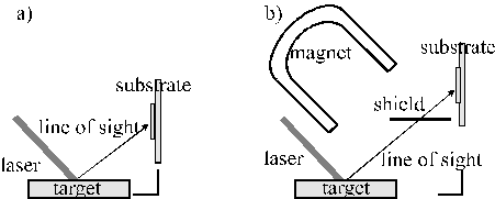
Figure 1.3: Different target to substrate set-ups: (a) off-axis set-up and (b) off axis set-up with magnetic field.
The first strategy for reducing the particulate density in the film involves an off-axis set-up, which has proven to be successful for the deposition of Ag-Co films.[17] A more involved arrangement incorporates a magnetic field (to deflect the plasma) in combination with an off axis set-up. This technique has been shown to be effective in the deposition of TiC.[18] The off-axis set-up is effective if the angular spread of the laser produced atomic and molecular species (in the ablation plume) is bigger than the angular spread of the laser produced particulates. The set-up with the magnet is reliant on the fact that the laser produced plasma (which includes molecular and atomic ions and electrons) can be deflected by a magnetic field while the ablated particulates are assumed to be electrically neutral and are not deflected by magnetic fields. Both techniques succeed in reducing the particulate density in the film but also cause a drastic reduction in the overall deposition rate. A much simpler route to reducing particulates in the deposited films involves heating the target to temperatures near to the melting point. This technique has been shown to be effective during deposition from metallic targets 16, and gallium and aluminium-gallium alloys.15 This technique can not, of course, be applied to deposition from target materials with very high melting temperatures (e.g. ceramics, graphite).
The possibility of large area deposition is very important if the technique is to be scaled up. Homogeneous deposition of YBCO on 3 inch diameter sapphire wafers has been reported 14 using an off axis rotating target and substrate assembly. YBCO deposition on 34 mm ´ 1 m stainless steel foils has been demonstrated also,13 but this still remains the Achilles' heel of the technique. Scaling up and developing a continuous process based on PLD has proven to be a laborious task to date.
As one can derive from this section, PLD is a technique that may be too difficult to implement as an industrial process. Nevertheless it has also been shown that the technique offers an unmatched versatility for depositing materials. In the next sections we will discuss the range of materials that are accessible with this technique.
1.2. Production of thin films via laser ablation
The production of different thin films via PLD has been illustrated in numerous papers, and here we can see the strength of the technique. PLD proves to be an excellent experimental technique for investigating the fundamentals of film deposition and the properties of new materials.
Table 1.3 summarises a few of the materials that can be deposited via laser ablation. Again, this list is not exhaustive. PLD is a rapidly developing field and the number of materials deposited by the technique is increasing rapidly; it is impossible to give a full review in this section. Rather, it might be viewed as a personal overview of the status of PLD growth of (possible) industrially important materials.
|
Class |
Material |
|
Oxides |
|
|
Nitrides |
|
|
Carbon based films |
|
|
Metals |
Table 1.3: Different materials deposited with PLD
Given the range of materials that it is possible to deposit with PLD it is beyond the scope of this overview to summarise specific deposition conditions for the different materials. The given list comprises superconducting materials (YBCO), wide band gap semiconductors (ZnO, TiO, Nitrides, Diamond), cold cathode field emitters (DLC, Diamond, carbon nanotubes), tribological materials (DLC, TiC) and metals. Given the simplicity of the process there are almost no restrictions on the target material to be used. PLD with liquid target materials has been illustrated 15,16,[33] and even PLD of solid nitrogen and methane has been probed experimentally.[34]
The other huge advantage of the technique relative to the other deposition methods is that it allows the possibility of introducing reasonable high pressures of background gas into the vacuum chamber. Such is often found to be necessary when depositing multicomponent films with specific stochiometry. It also enables creation of new materials during deposition, e.g. growth of nitrides or oxides from PLD of the respective single elemental materials in a background pressure of either oxygen or nitrogen. Such techniques can be developed further by introducing a pulsed flow of background gas (pulsed nozzle) or by depositing together with an ion beam arrangement.
Another strength of the technique can be seen when we look at the deposition of carbon films. By changing the deposition conditions, DLC (high vacuum, RT), diamond (O2 or H2 background gas and 500 °C) 28 and single wall nanotubes (He gas flow, Co catalyst and 1200 °C) 29 can be produced. PLD enables production of thin films of metastable materials like DLC, next to their more stable allotropes.
The deposition of Cu-Co Giant Magneto Resisting (GMR) thin films [35] and of thin films of SrBi2(Ta,Nb)2O9 used in the production of non-volatile Random Access Memory (RAM) [36] provide further illustrations of the use of PLD for the production of new materials.
1.3. New fields in the laser interaction with solids
The field of pulsed laser deposition is of course only a small part of a much larger field of interest, which is the interaction of laser light with solid materials. The next paragraphs give a few examples of fields related to laser ablation, along with a short discussion of their fundamentals.
1.3.1. Surface photochemistry
One important part of surface photochemistry is the photochemistry of adsorbate molecules on a solid surface. The subject of surface photochemistry with photons in the energy range of a few eV (comparable with the energy of a chemical bond) is subject to a large number of publications and has been reviewed by Polanyi et al.[37] The process of surface photochemistry can be divided in four different photochemical processes namely photodissociation (PDIS), photoreaction (PRXN), photodesorption (PDES) and photoejection (PEJ) in the adsorbed state. A schematic of the four processes is given in Figure 1.4.
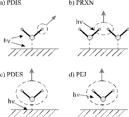
Figure 1.4: Different processes in surface photochemistry
PDIS refers to photodissociation of an adsorbed molecule, this may occur either directly or indirectly [38]. Direct absorption of a photon of sufficient energy results in a Franck-Condon transition from the ground state to an electronically excited repulsive or predissociative potential energy surface. If the energy state is repulsive, bond fission is instantaneous and the dissociation is favoured relative to other competing decay mechanisms like energy transfer to the substrate. Indirect photodissociation is a process whereby the substrate absorbs photons and causes fission of a bond in the adsorbate. The substrate can either absorb a photon by electronic excitation of defects, impurities or plasmons and then pass the energy via an electronic to electronic energy transfer to the adsorbate, or it can transfer an electron to an antibonding orbital of the adsorbate (called Charge Transfer/PDIS), thereby causing it to dissociate.
The PDIS process often results in the formation of photofragments whose translational energies are in excess of the energy required to surmount the activation barrier to chemical reaction in the adsorbed state. Under suitable conditions (i.e. where inter-adsorbate distances are small and the orientation favours the chemical reaction), either by high coverage or formation of islands, this can lead to reaction between a photofragment and a neighbouring adsorbate molecule. This process, initiated by absorption of photons by the adsorbate and involving adsorbate molecules only is called PRXN.
Photodesorption is defined as the process resulting in desorption of intact adsorbate molecules following absorption of photons by the substrate, whereas photoejection is reserved for the process resulting in desorption of intact molecules following photon absorption by the adsorbate. In the latter process the energy involved in the electronic excitation is converted into nuclear motion. Effects of the four different mechanisms are observed in adsorbates on metals, semiconductors and insulators as discussed in some length in reference 37.
1.3.2. Matrix Assisted Laser Desorption and Ionisation
Matrix Assisted Laser Desorption and Ionisation (MALDI) is an important and growing field. The technique involves irradiation of a laser absorbing matrix containing a small percentage of large molecules, e.g. biological molecules and polymers, which are transferred to the gas phase by desorption. This process is normally coupled to a mass spectrometer, which is used to measure the mass of the large molecules of interest. The technique is, to date, one of the most precise methods available for measuring the mass of biomolecules and polymers.
The fundamental theory of the technique is reviewed in the excellent papers of Garrison et al.,[39]-[41] which describe theoretical modelling of MALDI via Molecular Dynamics (MD) simulations. Former MD simulations [42] treated all of the atoms in the molecules, making the process very demanding computationally, since the upper limit of the time steps in the MD simulation were determined by the timescales of intramolecular vibrations. Only short time runs (45 ps) were thus affordable. The studies give information on a microscopic level only and cannot be readily extrapolated to larger systems.
The model discussed in the papers of Garrison et al. 39-41 do not take the individual atoms into account but assume that molecules can be treated as spheres. These spheres either expand or break down into smaller spheres when they absorb a laser photon reflecting, respectively, the laser induced vibrational excitation or breakdown of the molecule. Treating the molecules as spheres enables calculation of the dynamics of much larger systems over much larger time-scales compared to the former MD studies.
This 'breathing spheres' model has been extremely successful in qualifying the MALDI process. It predicts the sudden change in evaporation yield with increasing fluence that correlates with the onset of ablation (compared to surface evaporation) as observed in experiment [43] (see Figure 1.5). It also predicts a highly forward peaked ablation plume, which cools down rapidly, explaining why MALDI is successful in evaporation of large molecules without fragmenting them in the process.
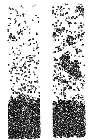
Figure 1.5: (a) and (b) are both snap shots of MD calculations for the same laser fluence and initial conditions, at the onset of the ablation regime. (a) Shows an evaporation regime where most of the ejected clusters are smaller than 4 molecules and (b) shows ablation behaviour where most of the clusters are bigger than 4 molecules. These figures illustrate the sharp transition between surface evaporation and ablation in MALDI.
1.3.3. Microshaping of Photonic Components
Microshaping of photonic components will be very important in the further development of the emerging field of photonics. One of the most important materials in photonics is fused silica, since it has a low absorption coefficient and is transparent over a broad wavelength range. Shaping of elements can be achieved via micromachining and etching [44],[45] but also by laser irradiation.[46] Laser irradiation of this wide bandgap material (9.3 eV) has some intrinsic problems, not least because of its low absorption cross section, but also associated with poor process control.
The recent development of bench-top F2 excimer lasers (l = 157 nm) offers a possibility of much improved process control.46 Holes drilled in fused silica with an F2 laser are incomparably smoother than those achieved using an ArF (l = 193 nm) laser; indeed their quality is high enough to be used in photonic applications.
1.3.4. Laser Ablation in space technology
Laser ablation offers potential important developments in space technology which probably started off as a tangent to the infamous ‘Star Wars’ project of President Ronald Reagan. Two different possible applications of high power lasers in space technology are given by Phipps et al.[47],[48] One is to clear near Earth space of debris, the other example involves use of laser ablation to launch satellites into low Earth orbit.
Anthropogenic near Earth space debris is an issue that is becoming a serious threat to the security of long term space missions. Almost a million pieces of debris have been generated during the 35 years of space flight. The most economical solution to this problem is to cause the debris to re-enter Earth’s atmosphere to burn up. Due to the number, speed and spatial distribution of the debris, an agile source of mechanical impulse is required. A combination of a high-resolution optical detection mechanism and a ground based laser system might provide the impulse to de-orbit the objects. Figures provided suggest that a 20 kW, 530 nm laser could clear the near Earth space of debris larger than 1 cm but less massive than 100 kg within 4 years.
Launching small objects into low Earth orbit is also considered to be a feasible application of laser ablation. The object accelerates via ablation of solid material of the satellite induced by a ground-based laser. This set-up can make the weight of the vessels much smaller since the need for a propelling rocket is removed, thus reducing the energy input required for putting small satellites into orbit. This is estimated to reduce the cost of launching 100-fold.
1.4. Scope of this thesis
This thesis concentrates on characterisation of the pulsed laser ablation processes of two materials, namely graphite and zinc oxide, and the study of the pulsed laser deposition of DLC (from graphite) and zinc oxide films.
Our study focuses on the detection and characterisation of the ablation plume via measurements of the optical emission and the charged components in the plume, thus providing a data set against which to test models for the ablation process. Such understanding of the processes governing laser ablation is fundamental to subsequent studies of the influence of the ablation / deposition process parameters on the properties of the grown films.
Graphite (DLC) and zinc oxide have been selected for their attractive properties, not only from an ablation viewpoint but also from a materials science point of view. DLC is currently used in the electronics industry as a wear resistant coating for hard disks. It is also a potential material for use as a cold-cathode field emitter. Zinc oxide thin films have a wide range of potential applications in the electronics industry. It is a wide band-gap semiconductor that can be doped easily with aluminium and gallium to produce transparent conductive films. The applications of lubricious zinc oxide coatings have also been investigated.
The ablation characteristics of the two different materials are also interesting from a fundamental point of view. The ablation of graphite is studied as an example of ablation of monocomponent materials. Its structural simplicity allows study of fundamental issues of laser ablation without ‘blurring’ from more complex phenomena related to multicomponent ablation. After this, the more complex ablation behaviour of zinc oxide has been studied. Fundamental issues relating to the ablation of two-component materials are addressed and explained.
The pulsed laser ablation and deposition of graphite has also been studied at a single wavelength (248 nm) with different laser pulse durations, namely 450 femtoseconds, 5 picoseconds and 35 nanoseconds. Laser excitation of the solid with these three different time scales (and thus intensities) reveals different ablation mechanisms and properties, which are reflected in the properties of the deposited films.
1.5. Conclusion
Laser ablation is, to date, one of the most versatile thin film deposition techniques with which to probe experimentally the production and properties of thin films. This experimental versatility runs counter to the usage of the technique in industry. Two practical deposition problems account for this lack of industrial usage. Laser ablation tends to produce not just a thin film, but also larger particulates which become incorporated in the film. This problem has been reported universally in deposition studies of all materials investigated. Scaling up of the technique is also proving difficult and, to date, most of the reported studies only involve use of small substrates (less than 1 inch diameter).
Research in laser ablation is at this moment focused on two areas, namely studies on the laser ablation process itself and of the film properties. Correlation of the two areas provides an integrated picture of the best process parameters to use when seeking to deposit a thin film with given properties. Next to this, although the general processes governing ablation are well understood, studies of the fundamentals of ablation of specific materials provide a more detailed and quantitative picture to strengthen the general theory, which will be discussed in Chapter 3.
This thesis emphasises this two-fold approach by seeking both qualitative and quantitative understanding of the laser ablation process of specific materials, correlating such results with the influence of the ablation conditions on the subsequent film deposition, and thereby providing a more profound understanding of the ablation process of the two materials, graphite and zinc oxide, discussed in this thesis.