Growth of Carbon Nanotubes
1. Introduction
Carbon nanotubes (CNTs) have the structure of graphite sheets that have been rolled up to form cylinders. They were first discovered by Ijima in 1991 [[1]] and since then a variety of methods have been developed for the synthesis of both single walled nanotubes (SWNTs) and multiwalled nanotubes (MWNTs). These include high pressure arcs, laser ablation and high pressure chemical vapour deposition (CVD) [[2]-[4]]. MWNTs can be deposited onto substrates coated with a suitable transition metal catalyst using plasma enhanced CVD techniques [[5]-[8]].
2. Experimental
Growth of carbon nanotubes was attempted using microwave activated chemical vapour deposition (MWCVD) in collaboration with N.V. Suetin (Moscow State University, Russia). Substrates consisted of a layer of Ni (~20 nm) deposited over a barrier layer (~200 nm), which was used to prevent the Ni from diffusing into the underlying Si substrate. The substrates used are summarised in Table 1.
|
Substrate Type |
Substrate |
Barrier Layer |
Catalyst layer |
|
1 |
Si |
Al2O3 |
Ni |
|
2 |
Si |
Ti |
Ni |
|
3 |
As substrate type 2 except
with patterned Ni layer |
||
Table 1. Substrates used during nanotube deposition experiments
Experiments were then carried out in which the substrates were exposed to a hydrogen plasma (in an attempt to sinter the Ni catalyst layer) prior to growth using various methane additions to the H2 plasma. Other experiments did not use a H2 plasma pre-treatment. All experimental conditions are outlined in Table 2.
|
Sample |
Substrate |
H2 Plasma |
Growth (CH4/H2
plasma) |
|||||
|
|
|
MW Power /W |
Pressure /Torr |
Time /min |
%CH4 |
MW Power /W |
Pressure /Torr |
Time /min |
|
NT 1 |
Type 1 |
1000 |
40 |
20 |
20 |
1000 |
40 |
10 |
|
NT 2 |
Type 1 |
- |
- |
- |
20 |
1000 |
40 |
10 |
|
NT 3 |
Type 1 |
1000 |
40 |
20 |
- |
- |
- |
- |
|
NT 4 |
Type 1 |
1000 |
40 |
10 |
10 |
1000 |
40 |
10 |
|
NT 5 |
Type 2 |
1000 |
40 |
10 |
20 |
1000 |
40 |
10 |
|
NT 6 |
Type 2 |
1000 |
40 |
10 |
20 |
1000 |
40 |
10 |
|
NT 7 |
Type 1 |
- |
- |
- |
20 |
1000 |
40 |
10 |
|
NT 8 |
Type 2 |
1000 |
40 |
10 |
20 |
1000 |
40 |
10 |
|
NT 9 |
Type 3 |
1000 |
40 |
10 |
20 |
1000 |
40 |
10 |
Table 2. Summary
of nanotube experiments.
Substrates were mounted on alumina, placed upon a Si wafer, and situated on the CVD chamber substrate cooler (see Figure 1). All experiments were undertaken with the substrate cooler in the same position relative to the plasma and samples were cooled in a H2 atmosphere for 10 min following growth.
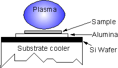
Figure 1. Diagram
showing sample mounting set-up.
3. Results
The deposition results will de discussed in terms of the effect of (i) H2 anneal, (ii) barrier layer type, (iii) substrate temperature (Tsub) and (iv) CH4 concentration on nanotube growth. Each aspect of the results will now be dealt with in turn, in addition to the analysis of films by laser Raman Spectroscopy. It should be noted that, in the following sections the word nanotube refers to the material deposited during experiments, and that nanotubes not been proved to be present (as would be possible by transition electron microscopy).
3.1. Effect of H2 Anneal
Two experiments were undertaken using two Type 1 substrates (Si/Al2O3/Ni), one with (NT1) and another without (NT2) H2 plasma pre-treatment. As shown by scanning electron microscopy (SEM) images in Figure 2, both samples yielded similar densely packed randomly orientated nanotube films. This suggests that the H2 pre-treatment had little effect in this case.
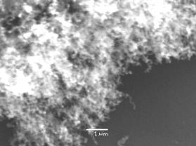
(a) (b)
Figure
2. SEM images of nanotubes grown on type 1 substrates (Si/Al2O3/Ni)
with (a) a H2 plasma pre-treatment, NT1, and (b) without any
pre-treatment, NT2. Conditions: as
given in Table 2.
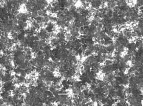
The H2 plasma pre-treatment was intended to sinter the Ni catalyst layer and form isolated areas (islands) of the metal on the substrate surface. One sample (NT3) was examined by SEM after H2 plasma treatment but there was no evidence of catalyst sintering. In addition, another sample (NT4) was exposed to a shorter (10 min as opposed to 20 min) H2 plasma pre-treatment prior to growth, and again no real change in the appearance of the nanotube film was seen by SEM (Figure 3). This sample was also grown at a reduced (10% rather than 20%) CH4 input concentration.
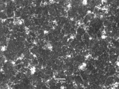
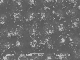
Figure 3. SEM image of nanotube film deposited on a type 1 (Si/Al2O3/Ni) substrate with a 10 min H2 plasma pre-treatment followed by 10 min growth time using a 10%CH4/H2 gas mixture (NT4). Conditions: pressure 40 Torr, MW power 1000 W.
3.2. Effect of Barrier Layer Type
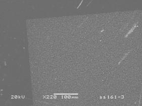
Figure 4 shows an SEM image of a nanotube film deposited on a substrate with a Ti barrier layer between the Si wafer and the Ni catalyst layer. It is clear that this substrate type yields smaller tubes which form a less densely packed film, compared with films deposited under similar conditions using a Al2O3 barrier layer (e.g. NT1, NT2 and NT4, as shown in Figures 2 and 3). In fact the film was so thin that it was invisible to the naked eye. In contrast, growth on type 1 substrates resulted in a visible film of soot-like appearance.
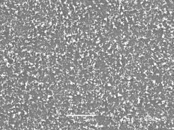
Figure 4. SEM image of a nanotube film on a type 2 (Si/Ti/Ni) substrate with a 10 min H2 plasma pre-treatment followed by 10 min growth time using a 20%CH4/H2 gas mixture (NT5). Conditions: pressure 40 Torr, MW power 1000 W.
3.3. Effect of Substrate Temperature
A repeat of the deposition experiment that yielded sample NT2 was run (NT7) with the substrate positioned closer to the plasma. These two experiments consisted of a 10 min growth period using a 20% CH4/H2 MW plasma (1000 W and 40 Torr) with no H2 plasma pre-treatment (using type 1 substrates with Al2O3 barrier layers). The latter sample (NT7) only had material deposited on the cooler parts of the substrate (i.e. those areas further away from the plasma), as illustrated by Figure 5(b)(ii). SEM examination of the areas of deposition for sample NT7 revealed a film identical in appearance to that seen for NT2.
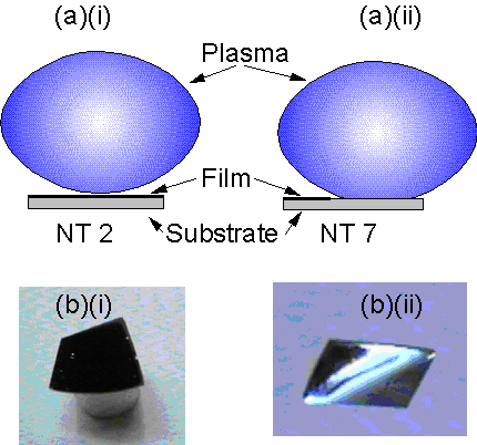
Figure 5. (a)
Diagrams of plasma-substrate interactions for (i) NT2 and (ii) NT7 and (b)
photographs of (i) NT2 and (ii) NT7.
Conditions: as given in Table 2.
In order to investigate the effect of Tsub on growth using substrates with Ti barrier layers, a type 2 substrate was placed in such a way as the substrate-plasma separation (and therefore Tsub) varied along its length (see Figure 6). After a 10 min H2 plasma pre-treatment this sample (NT8) was exposed to a 20%CH4/H2 plasma for 10 min. Subsequent SEM analysis showed that the deposit present in the hottest areas of the substrate (Figure 6(a)) was similar in appearance to that seen previously for type 2 substrates treated under similar conditions (see Figure 4). As Tsub decreased, the size of the tubular growths increased up to >10 mm in length (Figure 6(b) and (c)).
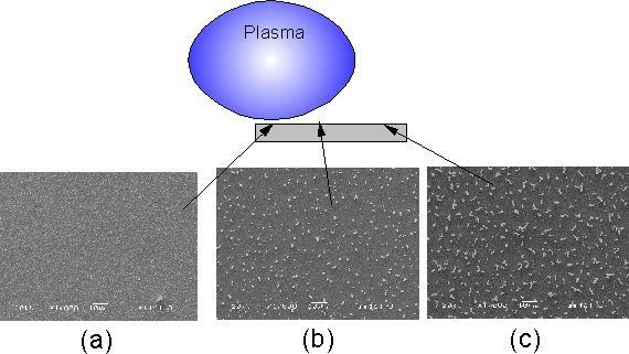 Figure 6. Diagram of substrate-plasma interaction during
deposition of sample NT8. SEM images of
areas of the substrate (as indicated) are also presented. Substrate used was of type 2 (Si/Ti/Ni) and
growth using a 20%CH4.H2 gas mixture (10 min) was
preceded by a 10 min H2 plasma treatment. Conditions: pressure 40 Torr, MW power 1000 W.
Figure 6. Diagram of substrate-plasma interaction during
deposition of sample NT8. SEM images of
areas of the substrate (as indicated) are also presented. Substrate used was of type 2 (Si/Ti/Ni) and
growth using a 20%CH4.H2 gas mixture (10 min) was
preceded by a 10 min H2 plasma treatment. Conditions: pressure 40 Torr, MW power 1000 W.
3.4. Effect of patterning of Ni layer
One substrate (type 3) consisted of Si covered with a Ti boundary layer (~200 nm) onto which Ni was deposited in square of dots. Figure 7 shows SEM images of the deposits resulting from a 10 min H2 pre-treatment followed by a 10 min growth period using a 20% CH4/H2 gas mixture. It is clear that the patterning has resulted in deposition of ill‑defined clumps of tubes, although it is not clear what material lies between these clumps.
(a) (b)
Figure 7. SEM images of deposit on type 3 (Si/Ti/Ni)
patterned substrate for (a) low and (b) high magnification. Growth (10 min) using a 20%CH4/H2
gas mixture was preceded by a 10 min H2 plasma treatment. Conditions: pressure 40 Torr, MW power
1000 W.
3.5. Raman Spectroscopy
Deposits grown on three type 1 (NT1,2 and 4) and a type 3 (NT9) substrates were analysed by laser Raman spectroscopy. Analysis was carried out with the laser beam incident to the substrate surface, using two different excitation wavelengths (514 and 785 nm). Spectra were collected from areas of high and low nanotube coverage. Such an area of high coverage is illustrated in Figure 3, while low coverage refers to areas with typically less than a monolayer of nanotubes present.
3.5.1. 514 nm Excitation
Figure 8 shows Raman spectra for typical growth on a type 1 substrate (sample NT1) for areas of (a) high and (b) low coverage. Each spectrum has been fitted using a linear baseline and Lorenzian lineshapes for the D-band (~1300 cm-1) and G-Band (~1580 cm‑1) and another unassigned band. The latter band could be linked with the Al2O3 barrier layer, as it was not needed for fitting spectra of samples grown on type 3 substrates. The prominent band evident at ~1000 cm-1 is the second order Si peak (due to the Si substrate).
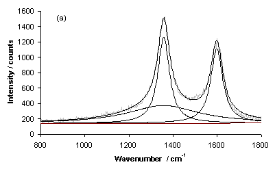
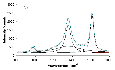
Figure 8. Laser Raman Spectra of sample NT1 (type 1 substrate) for an excitation wavelength of 514 nm for areas of (a) high and (b) low nanotube coverage. Each spectrum has been fitted using Lorenzian lineshapes (for the D and G-bands) and a linear baseline.
Curve fits allowed the intensities of the D-band (ID) and the G-band (IG) to be measured. As figure 9 shows, the ratio of ID/IG is seen to be greater for spectra taken of areas of high nanotube coverage than those of low coverage. This trend is seen for samples deposited on both type 1 and type 3 substrates.
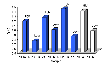
Figure 9. Plot of the intensity ratio of the D and G bands (ID/IG) for Raman spectra (514 nm) of samples grown using various type 1 (NT2 and 4) and type 3 (NT9) substrates. The nanotube coverage is given.
The full width at half maximum (FWHM) of the Raman G-band was also assessed for these samples. It was seen that the FWHM for spectra taken of samples grown on type 1 substrates was larger for areas of high, compared with low, nanotube coverage. However, as Figure 10 shows, this trend was reversed for deposits on type 3 substrates.
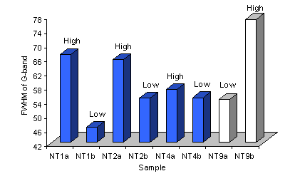
Figure 10. Plot of FWHM of the G-band for Raman spectra (514 nm) of samples grown using various type 1 (NT2 and 4) and type 3 (NT9) substrates. The nanotube coverage is given.
Previous work (using 514 nm excitation) has suggested that low ID/IG ratios and narrow (i.e. small FWHM) G-bands are suggestive of well-aligned carbon nanotubes [8]. The results presented within this section are clearly in agreement with this suggestion as the nanotubes within areas of low coverage are well aligned (horizontally, i.e. they lie flat on the substrate surface) and give lower ID/IG ratios and values of G-band FWHM than thicker nanotube films (i.e. areas with random nanotube orientations).
3.5.2. 785 nm Excitation
Figure 11 shows laser Raman Spectra for typical growth on a type 1 substrate (sample NT1) for areas of (a) high and (b) low nanotube coverage. The D-band (~1300 cm-1) and G-Band (~1580 cm-1) are both clearly evident and have been fitted using two Lorenzian lineshapes, in each case. A linear baseline has also been fitted to both spectra.
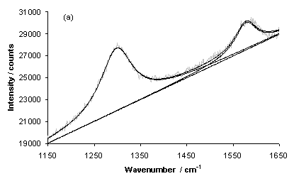
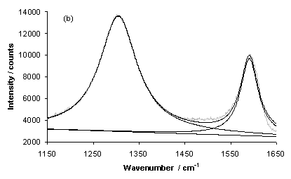
Figure 11. Laser Raman Spectra of sample NT1 (type 1 substrate) for an excitation wavelength of 785 nm for areas of (a) high and (b) low nanotube coverage. Each spectrum has been fitted using lorenzian lineshapes (for the D and G-bands) and a linear baseline.
It is clear that the spectrum for the area of low nanotube coverage has a baseline with a negative gradient, whereas the area of high nanotube coverage yields a spectrum with a linear baseline with a positive slope. This trend is also exhibited by other samples grown using type 1 (NT2 and 4) and type 3 (NT9) substrates, as illustrated by Figure 12. It is likely that the positive gradient observed for the baseline of spectra of areas of high nanotube coverage is due to photoluminescence caused by the random orientation of tubes, or the presence of amorphous carbon, within the film. This has been reported previously [8], although the work was carried out using an excitation wavelength of 514 nm.

Figure 12. Plot of the gradient of linear baselines fitted to Raman spectra (785 nm) of samples grown using various type 1 (NT2 and 4) and type 3 (NT9) substrates. The nanotube coverage is given in addition to the values for any data points extending past the axis limits.
It is clear from Figures 13 and 14 that, the trends in ID/IG and the FWHM of the G-band observed for Raman spectra taken at 514 are reproduced for an excitation wavelength of 785 nm. However, the values of ID/IG presented in Figure 13 are increased (~2 fold) compared with those for spectra recorded using a 514 nm laser (Figure 9). This indicates a greater sensitivity to the G-band for spectra collected using 785 nm, compared with 514 nm.
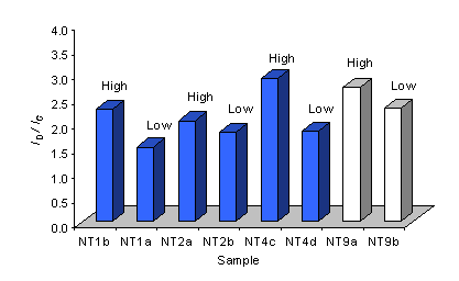
Figure 13. Plot of the intensity ratio of the D and G bands (ID/IG) for Raman spectra (785 nm) of samples grown using various type 1 (NT2 and 4) and type 3 (NT9) substrates. The nanotube coverage is given.
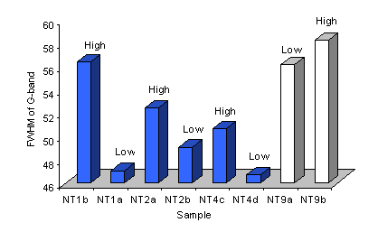
Figure 14. Plot of FWHM of the G-band for Raman spectra (785 nm) of samples grown using various type 1 (NT2 and 4) and type 3 (NT9) substrates. The nanotube coverage is given.
4. Conclusions
Nanotubes have been deposited on Si wafers coated with Ni, using both Al2O3 and Ti barrier layers. The use of Al2O3 barrier layers allowed the deposition of nanotubes of high density, whereas the Ti layered substrates yielded much lower nanotube coverage. It was also found that a H2 plasma pre-treatment was not necessary for the growth of a dense film of nanotubes on Si/ Al2O3/Ni substrates.
Raman spectroscopic studies have also been carried out and some correlations have been made between spectra and nanotube density and orientation. It should be noted that, all the work presented here should be considered as preliminary investigations carried out prior to much more extensive future work.