1. Introduction
Man throughout the ages has held diamonds in great esteem. In the following chapter the unique interest in, and properties of, this most prized gem will be discussed. The scientific and technological effort that has gone into producing synthetic diamond will also be examined, as will the applications of this ‘ultimate engineering material’. A discussion of two common diamond chemical vapour deposition (CVD) methods will be given, in addition to a brief review of the gas phase studies that have been conducted concerning such CVD processes. The topics of low temperature growth of diamond (LTGD) and the study of semiconducting diamond will also be introduced.
1.1. Diamonds in Nature
Diamond is formed within the asthenosphere, a band of molten rock between 75 and 120 miles below the surface of the earth. The crystals are then transported from the mantle to the Earth’s surface by explosive volcanic eruptions. After such volcanic activity, the molten diamond‑laden rock cools to form pipes of rock (Figure 1.1). This rock is named kimberlite, after Kimberley in South Africa where it was first discovered. In addition to diamond, kimberlite also contains rocks carried from the mantle called xenoliths. Xenoliths provide geologists with information about diamond growth conditions. These pipes then erode over millions of years resulting in diamond‑containing kimberlite being left relatively close to the surface of the Earth. The depth of erosion for three diamond producing kimberlite pipes are shown in Figure 1.1.
Figure 1.1. Schematic cross-section of a kimberlite
pipe (after Reference [1]).
1.2. Man and Diamond
It is almost certain that diamonds were discovered around 800 B.C. in Golconda, India. Diamonds were collected from rivers and flats where they had been deposited following erosion of a kimberlite pipe. India remained the world’s major diamond producer until the 1700s when its supplies began to dwindle. The discovery of diamonds in Brazil in 1725 led to this becoming the world’s principal diamond supplier until 1866 when diamonds were discovered in South Africa. In 1888 Cecil Rhodes consolidated four South African diamond mines into the syndicate that would become De Beers.
Up to this point diamonds had been mined from secondary deposits formed after the erosion of, and transport of material away from, kimberlite pipes. Following the discovery of diamonds in South Africa, geologists learnt that kimberlite pipes were the primary source of diamonds in the Earth’s crust, thus leading to the enormous modern diamond mines of Africa, Australia and Russia. Since the 1920s De Beers has controlled the production and marketing of diamonds on a global scale. Annually the company mines over half the world production of gem diamonds and also markets ~70% of all uncut diamonds [[2]].
1.3. Properties of Diamond
The driving force for the diamond mining discussed in the previous section was (and still is) the value placed on diamond as a decorative gemstone, due to its rarity, durability and beauty. The latter two qualities result from the exceptional hardness and refractive index of the material. As Table 1.1 shows, a number of the properties of diamonds can be described as exceptional.
|
Hardest known material (~90 GPa) |
|
Strongest known material, highest bulk modulus (1.2 ´ 1012 N m-2) lowest compressibility (8.3 ´ 10-13 m2 N-1). |
|
Highest room temperature thermal conductivity (2 ´ 103 W m-1 K-1). |
|
Good electrical insulator (room temperature resistivity ~1013 W cm). |
|
Wide bad gap (5.4 eV ) Þ broad optical transparency ( deep UV to far IR ) |
|
Very resistant to chemical corrosion. |
|
Biologically compatible. |
|
Exhibits low or 'negative' electron affinity. |
Table 1.1. Some of the
outstanding properties of diamond (adapted from Reference [3]).
1.4. Synthetic Diamond
The exceptional properties of natural diamond (illustrated by Table 1.1) have led to its industrial use in applications such as engraving, grinding and drilling. Such use requires a constant supply of diamonds of regular dimensions at as low a price as possible. These requirements have led to the quest for a synthetic route to diamonds. The first step along such a route was the discovery by Tennant in 1796 that diamond is composed entirely of carbon [[4]].
In fact, diamond and graphite are both allotropes of carbon differing only in their structure. Graphite is composed of planar sheets comprised of relatively strongly‑bound six‑member carbon rings. However, these sheets are only weakly bound to each other by van der Vaals attractions (bond strength = 7 kJ mol-1). On the other hand, the diamond structure is that of a lattice of tetrahedrally‑bonded carbon atoms [[5]]), as shown in Figure 1.2.

(a) (b)
Figure 1.2. Atomic structure
of (a) graphite and (b) diamond. The
weak van der Vaals bonding between adjacent graphite sheets is indicated by the
vertical dashed lines.
1.4.1. HPHT Synthesis
Attempts to synthesize diamond from graphite at room temperature and pressure proved unsuccessful. This was because, although the enthalpy of graphite is only 2.9 kJ mol-1 lower than that of diamond, a large activation barrier exists for the interconversion of the two carbon allotropes at room temperature [5]. Attempts to obtain diamond by simply exposing graphite to great pressure failed because this kinetic barrier increases with increased pressure [5]. The breakthrough came in 1954 when General Electric used a combination of high pressure and high temperature (HPHT) to obtain diamond from graphite [[6]]. This method required pressures and temperatures of the order of 150 kbar and 3000°C, respectively, as shown on the carbon phase diagram shown in Figure 1.3. However, the use of transition metal catalysts [5] has allowed diamond formation at lower temperatures and pressures (e.g. ~90 kbar and 2000°C).

Figure 1.3. Phase diagram
for carbon (after Reference [7]).
Since the 1950s HPHT processes have been commercialised by both Du Pont and De Beers for the purpose of industrial diamond production. Recently, a HPHT process has been reported which yields gem quality clear crystals from brown coloured natural diamonds [[8]].
1.4.2. Diamond Growth at Low Pressures
The first successful deposition of diamond at low pressures from the gas phase was reported by Eversole [[9]]. In this work, diamond seed crystals were heated to ~900°C in hydrocarbon gas at pressures <1 atm. Thermal decomposition of the feedstock gas led to addition of carbon to the seed crystal resulting in new diamond growth. Independent verification of these results was provided by Deryagin et al. [[10]]. Both experiments resulted in the co-deposition of diamond and graphite, however Angus et al. [[11]] reported the use of atomic hydrogen (produced from H2 by a tungsten filament) for etching this graphitic material leading to the use of a cyclic process of deposition and etching. A major advance was made when Derjaguin et al. went on to use atomic hydrogen during diamond deposition, leading to growth on non-diamond substrates by chemical transport within a closed system [[12]].
Then, in the early 1980s, researchers working at NIRIM in Japan reported the growth of diamond films on silicon substrates (maintained at ~900°C) using 1%CH4/H2 gas mixtures at pressures of ~30 Torr using hot filament [[13]] and microwave plasma [[14]] chemical vapour deposition (CVD) methods. These reports presented sufficient experimental details to enable others to reproduce their work, leading to an international explosion in diamond CVD research that continues to this day [[15]]. The NIRIM publications were also remarkable for their use of Raman spectroscopy for the unambiguous characterisation of the diamond films (see Section 2.3).
1.5. Diamond CVD Methods
Since the early 1980s, many methods for the growth of CVD diamond have been developed. All such methods require a route by which gaseous carbon‑containing precursor molecules are activated. Such activation can involve thermal methods such as hot filament (HF), DC, RF or microwave (MW) discharge, or a combustion flame (e.g. an oxyacetylene torch) [[16]]. The following sections will discuss the two most commonly used methods, i.e. HF and MW activated diamond CVD.
1.6. Hot Filament CVD
A schematic diagram of a HFCVD apparatus is shown in Figure 1.4. In this arrangement the process gas (usually 1%CH4/H2) is fed into the reactor chamber where it is activated by a coiled metallic filament (usually tantalum) maintained at ~2100°C. Diamond deposits on a substrate maintained at ~900°C placed ~5 mm from the filament. Exhaust gases are pumped from the chamber.
Figure 1.4. Schematic
diagram of a HFCVD system (after Reference 16).
The major advantage of such systems is that they are relatively simple (and therefore inexpensive). However, three major drawbacks of HF activated CVD are that (1) growth areas are limited to ~1 cm2, (2) material from the filament can contaminate deposited films and (3) the range of gases available for use in HFCVD is limited by the sensitivity of the filament to oxidising or corrosive species.
1.7. Microwave Plasma CVD
The original NIRIM design of a MWCVD apparatus is illustrated by Figure 1.5(a). In this configuration a quartz tube is placed within a waveguide. The substrate is placed on a heater at a position where a plasma is formed. The process parameters (i.e. pressure, gas mixture and substrate temperature) are essentially identical to those utilised during HFCVD, as is the average growth rate for films deposited under these conditions (for MW powers <1.5 kW).
Figure 1.5. Schematic diagrams of (a) NIRIM-type and
(B) ASTEX-type MWCVD apparatus (after Reference 16).
In 1988, a new design of MWCVD reactor was reported by Bachmann et al. [[17]]. A schematic of such an ASTEX-type reactor is presented in Figure 1.5(b). In this configuration microwaves are directed along a waveguide and are coupled into the chamber via an antenna. Microwaves pass through a quartz window and into the reactor. One advantage of this set-up is that the reactor walls are stainless steel, thus deposited films are free of Si and O contamination, which was a problem when using the quartz reactor tube in a NIRIM type reactor. The steel chamber also allows the use of higher microwave powers than the NIRIM design, with systems able to operate at up to 6 kW, thus delivering growth rates up to 10 mm h‑1.
Although MWCVD reactors are much more expensive (due to their complexity) than HF systems, they have become amongst the most widely used of all diamond CVD methods. This is due to a number of advantages. Firstly, the absence of a filament means that not only can a wide variety of gas mixtures be used (including oxygen containing molecules, as discussed in Section 1.14.1) but also no contamination of the growing film occurs. This is of particular importance for the growth of high quality diamond films for electronic applications (see Section 1.15). These advantages provide the main impetus for the use of an ASTEX MWCVD system for the work presented within this thesis, i.e. investigations of CH4/CO2 gas mixtures and also the growth of S-doped films for possible use in electronics.
1.7.1 Plasma Generation
A plasma is a ‘soup’ of neutral molecules, and atoms, ions and electrons. A microwave plasma is struck when electrons (either produced by a cosmic ray or intentionally by a spark) are accelerated within the oscillating electric field produced by the microwaves. These electrons are able to attain very high energies (>104 K), therefore when they collide with gas phase molecules they impart energy in the form of vibrational excitation. Successive impacts cause the molecule to either become ionised (thus freeing another electron) or dissociated. In such a manner the input gas mixture is activated, i.e. molecules are split up and gas phase chemical reactions are instigated. A stable plasma is attained when a steady state concentration of electrons is present. The plasma formed within an ASTEX-type MWCVD reactor has the appearance of a glowing ball, due to the optical emission caused by electronically excited gas phase species relaxing down to lower energy levels.
1.7.2. Plasma properties
Plasmas, in general, are characterised by their electron, ion and neutral species temperatures, in addition to their degree of ionisation (i.e. number density ratio of charged and neutral species). MW plasmas operating at ~40 Torr and powers of ~ 1 kW are generally thought of as having electron temperatures of the order of ~105 K (i.e. ~10 eV). As already stated, ions and neutrals are only able to obtain thermal energy from collisions with either each other or highly energetic electrons, and thereby have much lower temperatures (of the order of 1000‑2000 K, i.e. ~0.2 eV).
An upper limit for the degree of ionisation of 4´10-7 has previously been calculated [7] for a 2.45 GHz microwave generated plasma (for a pressure of 20 Torr and assuming a Tgas of 1400 K). It is therefore clear that such a MW plasma, as used for all the experiments presented in this thesis, can be considered to be very weakly ionised. The applied microwave energy can therefore be considered merely to heat the input gas mixture (via highly energetic electrons) and thus activation of the feedstock is largely thermal.
1.8. The Chemistry of Diamond CVD
A detailed description of the chemical processes governing diamond CVD can be found within Reference [18], however a brief account will be given within this section. A schematic representation of the CVD process is shown in Figure 1.6, in which a reactant gas mixture is activated (e.g. by HF or MW). The resulting species then undergo reaction and diffuse to the substrate surface. Nucleation of microscopic diamond crystals then occurs either on a diamond (homoepitaxy) or non-diamond (heteroepitaxy) substrate.
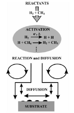
Figure 1.6. A schematic
diagram of the diamond CVD process (after Reference 18).
The activation and reaction of the input gas mixture will be discussed in the following sections in terms of the diagnostic techniques used to determine gas phase species concentrations. The nucleation of diamond and the early growth of the film will then be discussed within Section 1.12.
1.8.1. Diamond Growth Precursor Species
The question of which C containing gas phase species is the major diamond precursor has been of great interest, both from academic and process optimisation standpoints. The observation that MW and HFCVD both deliver diamond films at similar growth rates indicates that the diamond precursor is likely to be a neutral species.
Harris et al. reported that modelling of gas phase reaction kinetics and consideration of measured diamond growth rates suggested that CH3 and C2H2 were possible diamond precursor species [[19]]. Table 1.2 shows the results of isotope labelling studies in which a 2:1 mixture of 13C methane and 12C acetylene was introduced into a HFCVD reactor in such a way as to minimise isotopic scrambling between the two species [[20]]. The 13C mole fractions of the resulting (homoepitaxial and polycrystalline) films were determined by Raman spectroscopy and were found to be very similar to those of the input CH4. It was assumed that 13CH4 and 13CH3 were in equilibrium, therefore CH3 was concluded to be the diamond precursor species. Similar results were obtained by Johnson et al. [[21]] using a cavity plasma reactor, as shown in Table 1.2.
|
|
|
13C Mole Fraction (%) |
||
|
CVD Method |
Film Type |
Film |
CH4 |
C2H2 |
|
Hot-filament |
Polycrystalline |
58.2 ± 3.6 |
61.6 ± 5.5 |
32.4 ± 5.6 |
|
Hot-filament |
Homoepitaxial |
56.8 ± 1.2 |
58.6 ± 5.4 |
34.9 ± 5.3 |
|
Microwave |
Polycrystalline |
77 |
83 |
29 |
Table 1.2. Summary of results for isotopic labelling
experiments carried out in HF [20] and MWCVD [21] reactors (after Reference 18).
Lee et al. [[22]] carried out a set of experiments in which jets of (1) CH3 and H2, (2) CH3 and H and (3) C2H2 and H were directed at diamond seed crystals. Epitaxial diamond growth on these crystals was only observed for incident jets of CH3 and H, whereas replacing CH3 with C2H2 resulted in a largely graphitic deposit. This study and a number of others involving a wide variety of CVD diamond deposition methods (see references 18 and [23] and references therein) have concluded that CH3 is the major diamond precursor in low-pressure low‑power diamond CVD reactors (e.g. HF, MW and flame CVD). However, it should be noted that C2, or C atoms may be the dominant growth species at higher powers (i.e. >5 kW) in, for example, a DC arc jet reactor [[24],[25]].
1.9. Gas-phase Diagnostics of HFCVD
The gas phase environment of a HFCVD reactor was first probed by Kawato and Kondo, as reported in 1987 [[26]]. They used gas chromatography to sample gas from the reactor exhaust line, in which they detected CH4, C2H4, C2H2, H2 and CO (for an H2/CH4/O2/Ar input gas mixture). The majority of the input carbon was found to be converted to C2H2 with measured CH4 concentrations ~5% of the input concentration.
Subsequent investigations looked at the variation in gas phase species concentrations with CH4/H2 ratio, filament temperature (Tfil) and distance from the filament (d). The variation of gas temperature, Tgas, with d is also of great importance to the understanding of the gas phase chemistry of HFCVD. These investigations, along with computer modelling studies, of HFCVD processes will be the subject of the following sections, which serve as background for the results presented in Sections 6.5-6.7.
1.9.1. The Effect of Filament Temperature
Celii and Butler showed that (for an input gas mixture of ~1%CH4/H2) increasing Tfil caused an increase in the intensity of the resonance enhanced multiphoton ionisation (REMPI) signal due to CH3 [23]. A similar result was also obtained by Corat and Goodwin who used REMPI to probe CH3 in the vicinity of the substrate and mass spectrometry to measure CH4 and C2H2 mole fractions ([CH4] and [C2H2]) present in the exhaust line [[27]]. As Figure 1.7 illustrates, increasing Tfil was seen to cause a decrease in [CH4] but an increase in [C2H2] and the CH3 REMPI signal.
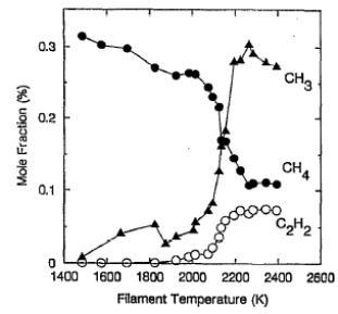
Figure 1.7. Measured CH3
REMPI signal (arbitrary units) and CH4 and C2H2
mole fraction versus Tfil (as measured by optical
pyrometry). Conditions: 0.5%CH4/H2,
pressure 26 Torr and Tsub = 1000 K (after Reference 27).
In addition, Smith et al. have reported increased REMPI signals for both CH3 and H with increased Tfil [[28]]. Molecular beam mass spectrometry (MBMS, as discussed in section 1.11) studies by Hsu et al. have also shown similar behaviour of [H] with increasing Tfil [[29]].
1.9.2. The Effect of Input Gas Mixture
Toyoda et al. [[30]] determined CH3 number densities (for d = 0.7 cm) using UV absorption spectroscopy. It was found that the measured CH3 densities were nearly identical for either C2H2 or CH4 input hydrocarbons, when an equivalent amount of carbon was used. A similar result was reported in the work of Rego et al. [[31],[32]] in which MBMS measurements were made (as a function of Tfil) for input gas mixtures of 1%CH4/H2, 0.5%C2H2/H2 and 0.5%C2H4/H2. As Figure 1.8 shows, the species mole fractions measured in the vicinity of the filament at Tfil values used during growth of good quality CVD diamond (i.e. ~2400 K) are strikingly similar for all three input gas mixtures.
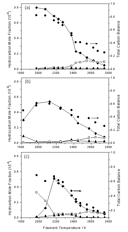
Figure 1.8. MBMS measured mole fractions of CH4
(®), C2H2
(£) and C2H4
(▲) sampled at d = 5 mm presented as functions
of Tfil, for HF activated (a) 1%CH4/H2,
(b) 0.5%C2H2/H2 and (c) 0.5%C2H4/H2
gas mixtures. The total carbon mass
balance is also presented on each plot (●). Conditions: pressure 20 Torr, total gas flow 100 sccm (adapted
from Reference 32).
Hsu et al. have shown [[33]] that the MBMS mole fractions of CH4, C2H2, and CH3 measured at the substrate all increase, while [H] decreases, with increased input CH4 for 0.5-7%CH4/Ar/H2 gas mixtures. In addition, Smith et al. have reported an increase in CH3 REMPI signal for increased %CH4 in HF activated CH4/H2 gas mixtures [28].
1.9.3. Species Concentrations: Variation with Distance from Filament
Zare et al. have used cavity ring-down
spectroscopy to make CH3 column density measurements as a function
of d (radial distance from filament) [[34],[35]]. Their results are in good qualitative
agreement with those of Smith et al, whose REMPI measurements of 1%CH4/H2
and 0.5%C2H2/H2 HF‑activated gas
mixtures are presented in Figure 1.9.
The observed trends for both gas mixtures are seen to be remarkably
similar.
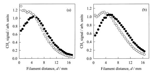
Figure
1.9. CH3 REMPI signals (![]() ) measured as a function of d
using (a) 1% CH4 in H2 and (b) 0.5% C2H2 in H2 gas mixtures, 20 Torr pressure, 100 sccm gas flow rate and Tfil = 2475 K. The open symbols (¡) show the d dependence of the total CH3 relative number density obtained by scaling the
measured REMPI signals with the appropriate temperature dependent sensitivity
factors (after Reference 28).
) measured as a function of d
using (a) 1% CH4 in H2 and (b) 0.5% C2H2 in H2 gas mixtures, 20 Torr pressure, 100 sccm gas flow rate and Tfil = 2475 K. The open symbols (¡) show the d dependence of the total CH3 relative number density obtained by scaling the
measured REMPI signals with the appropriate temperature dependent sensitivity
factors (after Reference 28).
1.9.4. Gas Temperature: Variation with Distance from Filament
Harris et al. have reported thermocouple measurements of Tgas for a ~0.3%CH4/H2 gas mixture at 20 Torr as a function of d. A precipitous drop in temperature was measured within 1 mm of the filament [19]. Similar results have also been obtained by Chen et al. [[36]] and Smith et al. [28] using H2 rotational temperatures measured using coherent anti-Stokes Raman scattering (CARS) and H atom REMPI Doppler profiles, respectively. The results of Smith et al. are presented in Figure 1.10 with the solid line through the points derived from a 2D computer simulation of the temperature profile in a HFCVD reactor [[37]].
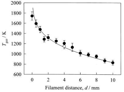
Figure
1.10. Local gas temperatures in 20 Torr of pure H2 with Tfil = 2360 K, as deduced from analysis of the H atom
2s ¬ 1s two photon Doppler lineshapes (![]() ), plotted as a function of d. The open circle shows the rotational
temperature deduced by simulating the contour of the measured 2 + 1 REMPI
spectrum of the CH3 origin band at d = 4 mm, and the solid line is a 2D computer simulation of Tgas
(after Reference 28).
), plotted as a function of d. The open circle shows the rotational
temperature deduced by simulating the contour of the measured 2 + 1 REMPI
spectrum of the CH3 origin band at d = 4 mm, and the solid line is a 2D computer simulation of Tgas
(after Reference 28).
1.9.5. Modelling Studies
Various groups have undertaken computer modeling
studies of the HFCVD process in order to gain insight into the chemical
reactions taking place. Harris et
al. [19] reported calculations of the time history for
species mole fractions using a detailed chemical kinetics model [[38]]
assuming isothermal conditions at 2000 K.
Goodwin and Gavillet carried out more detailed
calculations involving both the effects of reaction kinetics and species
transport [[39]].
These simulations were based on a 1D model in which gas passes through a
porous, infinite radius plate (i.e. the filament) at a temperature of Tin,
is transported downwards towards a substrate (at a temperature of Tsub)
[[40]]. Kinetic, thermodynamic and transport
properties are evaluated using the CHEMKIN II program suit [[41]] and related Transport packages [[42]],
respectively. Figure 1.11 presents
plots of species mole fractions calculated for the conditions of the
experimental measurements of Harris et al. [19]. To allow
comparison with experiment, the results are plotted as a function of distance
from a substrate, z, with a filament positioned at z = 0.5
cm. A good agreement with experiment
was reported for both this, and a simulation based on the experimental results
[[43]]
of Celii et al.. One important
conclusion reached was that homogeneous recombination of H can be neglected in
HFCVD systems, therefore H atoms are freely able to diffuse to the substrate.
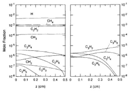
Figure
1.11. Species mole fraction profiles calculated for simulating experiments of Harris
and co-workers [19]. Plots are
presented as functions of distance from substrate, z, with the filament
positioned at z = 0.5 cm (after Reference 39).
Dandy and Coltrin reported [[44]] similar calculations in which gas
phase [[45]] and
surface [[46]] reaction mechanisms were used to
simulate the results obtained by Hsu [33] (obtained using MBMS with gas sampled through a hole
in the substrate, as described in Section 1.11). The results of these simulations are presented in Figure 1.12 in
which the inlet gas temperature is set at (a) 1720 K (i.e.
900 K lower than the experimental Tfil) and (b)
2620 K (i.e. Tin = experimental value
of Tfil). It is clear
that this variation of Tin has relatively little effect on
the agreement between the calculated and experimental species mole fractions.
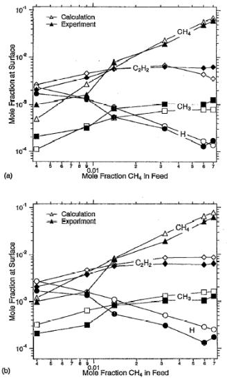
Figure
1.12. Numerical and experimental [33] results for gas-phase species distributions at the
substrate. Numerical results are presented for two values of Tin
; (a) 1720 K, (b) 2620 K (after Reference 44).
Further simulations have also been carried out by
Tsang et al. [[47]],
using the approach outlined above. In
this work the CHEMKIN II suit of computer packages [41] was used along with the SENKIN code [[48]]
to calculate the gas composition at the filament. The SPIN code [[49]]
was then used to calculate H and CH4 mole fractions at a distance of
2 mm from the filament, for a range of Tfil. The calculations were then compared with
MBMS measurements made using a probe to sample gas from a position 2 mm from
the filament and parallel to the substrate (which is positioned 5 mm from the
filament). Two values of Tin
were used, Tfil–500°C and Tfil–900°C with
little difference seen between the results obtained using either. However, the input mole fraction of H was
found to be a crucial simulation parameter, suggesting that H atoms produced
heterogeneously on the surface of the filament [[50]]
drive the gas phase chemistry of HFCVD.
1.10. Gas-phase Diagnostics of MWCVD
This section will serve as background for all the investigations of MWCVD presented within this thesis. A general discussion of gas phase diagnostics carried out for various hydrocarbon/H2 CVD diamond gas mixtures will be presented with further discussions of H/C/O and H/C/S containing gas mixtures contained within Sections 1.14 and 1.17, respectively.
1.10.1. Species Concentrations
The gas phase chemistry of diamond MWCVD was first investigated by Saito et al. [[51]] who used optical emission spectroscopy (OES) to detect the presence of electronically excited H, CH and CH2 within a 1%CH4/H2 microwave plasma operating at 20 Torr. Later Mitomo et al. [[52]] used Fourier transform infrared (FTIR) spectroscopy to make measurements of CH4, C2H2 and C2H4 concentrations for a variety of H/C and H/C/O containing input gas mixtures. As Figure 1.13 shows, the results obtained from input mixtures of H2 and CH4, C2H2 and C2H4 are remarkably similar. They also found that measurements of CH3OH/H2, C2H5OH/H2 and CO/H2 plasmas gave similar concentrations of CH4, C2H2, C2H4 and CO. In addition it was shown that increased addition of O2 to a 1%CH4/H2 plasma caused a drop in CH4 and C2H2 concentrations.
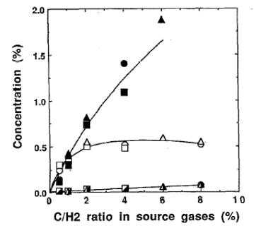
Figure 1.13. Concentration
of stable compounds in the plasmas CH4/H2, C2H2/H2
and C2H2/H2 as a function of C/H2. Source gas mixture: CH4/H2:
(![]() )
%CH4, (
)
%CH4, (![]() )
%C2H2, (
)
%C2H2, (![]() ) %C2H4; C2H4/H2:
(
) %C2H4; C2H4/H2:
(![]() )
%CH4, (
)
%CH4, (![]() )
%C2H2, (
)
%C2H2, (![]() ) %C2H4; C2H4/H2:
(
) %C2H4; C2H4/H2:
(![]() )
%CH4, (
)
%CH4, (![]() )
%C2H2, (
)
%C2H2, (![]() ) %C2H4 (after Reference 52).
) %C2H4 (after Reference 52).
MBMS measurements of gas sampled through an orifice in a substrate were reported by Hsu [[53]] using identical apparatus to that used to make measurements of hot filament activated gas mixtures (see Reference 33 and Section 1.19). In this work the change in concentration of H2, Ar, C2H2, CH4, H and CH3 were investigated as a function of CH4 fraction (0.2-3%) in the input CH4/Ar/H2 gas mixture. It was found that increased input %CH4 caused increases in the detected concentrations of all three hydrocarbons, whereas H2, H and Ar concentrations remained relatively stable. Hsu also made a comparison between species concentrations measured with MW and HF activation of a 0.35%CH4/Ar/H2 gas mixture at 20 Torr and found these to be in good agreement (see Table 1.3). The conclusion of this work was that the hydrocarbon chemistry in MWCVD (as in HFCVD) is strongly dictated by neutral-neutral reactions and the role of the plasma is to dissociate hydrogen molecules without having to raise Tgas significantly, as previously suggested by Okeke and Stori [[54]].
|
Activation |
H |
CH3 |
CH4 |
C2H2 |
|
Microwave Plasma |
1.21´10-3 |
1.62´10-4 |
1.30´10-3 |
9.47´10-4 |
|
Hot Filament |
1.18´10-3 |
2.03´10-4 |
9.89´10-4 |
2.03´10-3 |
Table 1.3. Comparison of
mole fractions measured by MBMS in microwave plasma and hot filament systems at
a pressure of ~20 Torr and Tsub of 800°C. Conditions: gas mixture 0.35%CH4/Ar/H2,
microwave power 800 W, Tfil = 2600 K (after
Reference 53).
Later, McMaster et al. [[55]] made similar MBMS measurements of 0.35-7.5%CH4/H2 and 0.24‑3.7%C2H2/H2 microwave activated gas mixtures and showed that species mole fractions (measured at the substrate) are generally independent of input hydrocarbon (as shown in Figure 1.14). The same conclusion was reached by Leeds et al. [[56]] who made MBMS measurements by sampling gas from the side of the plasma ball rather than at the substrate.
Figure 1.14. Mole fractions
of species measured in a MWCVD reactor as a function of carbon mole fraction in
the input gas mixture, Xc, for (a) C2H2/Ar/H2
and (b) CH4/Ar/H2.
Conditions: microwave power 850 W, pressure 20 Torr, Tsub
= 825°C (after Reference 55).
An increase in CH3 mole fraction with increased input methane to a CH4/H2 gas mixture (as determined by UV absorption spectroscopy) has also been reported by two other groups [[57],[58]].
1.10.2. Temperature Measurements
Chu et al. [[59]] made measurements of the gas kinetic temperature in a 1%CH4/H2 dc hollow cathode discharge using the relative line intensities of H2 and CN (N2 present as an impurity in CH4 gas supply) optical emissions. These measurements were confirmed by laser induced fluorescence (LIF) spectroscopy and it was shown that Tgas varied linearly with pressure, discharge power and distance from the anode. Similar results were also obtained by Lang et al. [[60]] who derived Tgas from Doppler broadening of H2 and Ha lines as measured by OES.
In addition, measurements of Tgas (denoted Tg) within a 100%/H2 MW plasma were made by Gicquel et al. [[61]]. As shown in Figure 1.15, the H atom temperature, TH(K), obtained by measuring the Doppler broadening of the two-photon allowed LIF (TALIF) signal, agrees well with the ground electronic state rotational temperature of H2, TH2(X), as measured by CARS. Figure 1.15 also illustrates the point that the temperature gradients present within such a MW plasma are much more shallow than those present within a region close to the filament in a HFCVD reactor (as shown in Figure 1.10).
Figure 1.15. Axial
distribution of the rotational temperature of ground electronic state hydrogen
(TH2 (X)) and of the ground state H-atom temperature (TH (K)). Plasma conditions: power density 9 W cm-3,
MW power 600 W, pressure 19 Torr, interaction with an untextured diamond
surface positioned at 0 mm (after reference 61).
More recently, Leeds et al. reported Tgas measurements of a 2%Ar/H2 MW activated gas mixture obtained by measuring the MBMS signal due to Ar sampled from the side of the MW plasma ball. This signal had been previously shown to scale as Tgas-1.6. As Figure 1.16 shows, these measurements are in good agreement with those of Lang et al. [60] (when the latter are scaled for the conditions of the MBMS measurements).
Figure 1.16. Gas
temperature determined in a 2%Ar/H2 plasma. ![]() : the Ar signal (counts per second, c s-1)
measured by the mass spectrometer.
: the Ar signal (counts per second, c s-1)
measured by the mass spectrometer. ![]() gas temperature calculated from the Ar signal. ·: results of Lang et al.
[60], which have been extrapolated to the MBMS measurement
process conditions. Conditions:
Pressure 20 Torr, Tsub ~1000°C, gas probed from a point ~15 mm from center of reactor (after
Reference 56).
gas temperature calculated from the Ar signal. ·: results of Lang et al.
[60], which have been extrapolated to the MBMS measurement
process conditions. Conditions:
Pressure 20 Torr, Tsub ~1000°C, gas probed from a point ~15 mm from center of reactor (after
Reference 56).
1.10.3. Modelling Studies
McMaster et al. [55] performed numerical simulations of species mole fractions measured by MBMS in a MWCVD reactor (as discussed in Section 1.10.1) using the same model previously employed to investigate HFCVD (as discussed in Section 1.9.5). Their gas-phase reaction mechanism [46] incorporates the kinetics of 34 homogeneous reactions; no plasma effects (e.g. ion-neutral or electron-neutral reactions) are included. Although this mechanism was used successfully to predict the near surface composition in a HFCVD reactor, the agreement obtained with measurements made during MBMS was generally not quantitative. This lack of success may have been due to the difference in Tgas gradient within a microwave plasma when compared with that present within the region of a hot filament.
1.11. Molecular Beam Mass Spectrometry
This section will present a more detailed discussion of the MBMS technique, as applied to gas phase measurements of diamond CVD environments, and will serve as a general introduction to the experimental measurements presented within this thesis (see Section 3.5).
Mass spectrometry was amongst the first gas phase diagnostic technique to be applied to diamond CVD due to its ability to measure several different species simultaneously. However, there is a major problem with the implementation of such a method, in that it is necessary to sample gas from a CVD chamber at a pressure of ~20 Torr while still maintaining a pressure within the mass spectrometer of ~10-6 Torr. The simplest way to achieve this is to sample gas through a capillary tube (see work of Corat and Goodwin in Section 1.9.1), although reactions within the tube mean that radical species are not detectable by this technique.
This limitation can be overcome by the use of a two stage differential pumping system in which gas is sampled from the CVD chamber via an orifice. Gas passing through this orifice experiences a pressure differential (a drop of ~10000 fold) and undergoes adiabatic expansion forming a molecular beam in which chemical reactions are effectively frozen out. The molecular beam then passed through another orifice into a mass spectrometer. The important factors to consider when designing such a system are given below (see also Reference [62]):
a1 = Diameter of the first sampling aperture between the plasma region and the first pumping stage.
a2 = Diameter of the second sampling aperture between the first and second pumping stages.
S1 = Net stage one pumping speed close to the first aperture.
S2 = Pumping speed in second stage (mass spectrometer) close to the second aperture.
Figure 1.17. Diagram illustrating two stage
differential pumping problem.
The conductance of an aperture (in the molecular flow region) for N2 is given by:
C = 11.6 A litres sec-1, where A is the area of the aperture in cm2 (e.g. for the first aperture A1 = (π a12) / 4 )
Therefore for a pressure p0 in the sampling region the pressure p2 in the mass spectrometer is given by;
p2
= (11.62 p0
A1 A2) / (S1 S2) Equation
1.1
and the pressure p1 in the first stage by;
p1 = (11.6 p0 A1) / S1 Equation 1.2
In order to obtain meaningful sampling from the plasma region it is essential to ensure that a molecule/atom can leave the source and enter the first stage without making any collisions. This is achieved by putting;
λ0 / a1 > 1 Equation 1.3
where λ0 is the mean free path at p0 (e.g. ~450 mm at a pressure of 20 Torr).
It is also necessary to minimise the interaction between the sampled species and the gas in the first stage. This is done by limiting the path length d in the first stage;
λ1
> 10 d Equation
1.4
Using such considerations, Hsu and Tung [[63]] constructed a MBMS apparatus to sample gas through an orifice in a substrate placed within a CVD chamber in which either HF or MW activation of the input gas mixture could be employed (see Figure 1.15). This apparatus was used to make measurements of both stable and radical species for a variety of input gas mixtures [29,33,53,55], as discussed in Sections 1.9 and 1.10. One important consideration is the energy used to ionise the species in the molecular beam. This energy should be minimised so as to prevent fragmentation of species, thus leading to the use of the threshold ionisation technique (see also Section 3.7.2).

Figure 1.18. Schematic diagram of the MBMS system
used for studying diamond CVD. Three
stages of differential pumping are used for gas sampling. The third stage is a shroud that surrounds
the electron-ioniser region. In the
process chamber reactive species can be formed either with a hot filament or a
plasma ball generated by microwave heating (after Reference 63).
Later work in Bristol used MBMS to sample gas directly from the plasma, thus probing the gas phase chemistry in isolation, with minimum perturbation from gas-surface reactions. We have used this powerful technique to obtain absolute mole fractions of the gas phase species present in both hot filament [31,[64]-[67]] and microwave systems [7,56,[68]].
1.12. Nucleation and Growth of the Diamond Film
In order for diamond crystals to nucleate and grow a suitable substrate must be chosen for diamond CVD. The use of a single crystal diamond substrate results in homoepitaxial (i.e. diamond on diamond) growth whereas a non-diamond substrate requires heteroepitaxial growth to occur. Diamond films will only grow on, and adhere to, substrates that are able to form a surface carbide layer, such as Si, Mo and W, however the reactivity of a substrate cannot be too high otherwise carbon will dissolve into it and no growth will result [16]. It has been found that pre-treatment of the substrate is necessary in order to obtain a nucleation density sufficient to allow the growth of a continuous diamond film [[69]]. This pre-treatment often takes the form of abrasion of the substrate surface with diamond grit (<10 mm). Another obvious requirement is that the substrate must be able to withstand the temperatures (i.e. Tsub ~ 900°C) required for diamond CVD processes, as discussed further in Section 1.14.
Once nucleation of carbon has occurred then homoepitaxial diamond growth proceeds. The individual crystals become progressively larger and eventually grow into each other, leading to characteristic columnar growth (in the case of non-diamond substrates), as shown in Figure 1.19(a). The surface morphology of a film grown on a non-diamond substrate depends on the relative growth velocities of the different diamond crystal planes. In fact, the facets that appear on a crystal are those for which the normal growth velocity is the slowest [69]. In practice it is observed that the (110) is the fastest growth direction, whereas growth rates for the (111) and (100) directions are approximately equal.
The type of facets that make up a CVD diamond film can be governed by controlling deposition process conditions such as the substrate temperature or the carbon concentration present in the input gas mixture. Therefore, if the (100) direction predominates, the surface will be made up of triangular (111) facets (Figure 1.19(b)), whereas if (111) growth is prevalent, the surface will be made up of cube-like (100) crystallites (Figure 1.19(c)). Growth on diamond substrates follows the direction of the substrate.
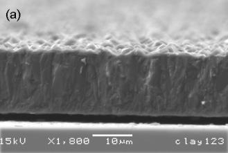
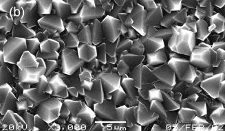
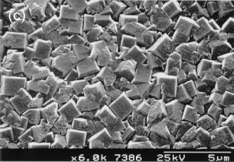
Figure 1.19. Scanning electron micrographs of MWCVD
grown diamond films deposited on Si substrates. Images are of (a) film cross section, (b) surface of films
displaying predominantly (111) facets and (c) surface of film displaying
predominantly (100) facets (Figure 1.19(c) after Reference [70]).
During diamond deposition from a 1%CH4/H2
gas mixture, the growing surface is believed to be H-terminated, which is
necessary to prevent graphitisation of the surface. Therefore, growth only occurs at sites without an H present, i.e.
a dangling bond, which can then be attacked by a CH3 radical [16,18]. If a
continuous diamond crystal is to grow it is necessary for this carbon species
to migrate across the surface to a step site [[71]]. It has been reported that the barrier to
such migration is lower for CH2 than for CH3 [[72]],
which could be formed if one of the methyl hydrogens is removed (either by an
adjacent dangling bond, or a gas phase H atom).
Further insight into the growth of CVD diamond films
was provided by Corat et al. [[73]] who collated growth rate results
from a number of CVD diamond deposition experiments using C/H, C/H/Cl and C/H/O
containing input gas mixtures. All
these experiments were found to have a similar temperature dependence of growth
rates (each dataset normalised to a value of 1 for Tsub =
1000 K), when presented as an Arrhenius plot (Figure 1.20). As Figure 1.20 shows, two activation
energies were found for high (600-900°C) and low (<600°C) Tsub. It was concluded that the incorporation of CH3 into
the diamond film growth surface might be the rate limiting growth step at high Tsub. However, other reported activation energies
[[74],[75]]
do not agree well with the results of Corat et al.
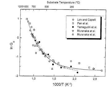
Figure 1.20. Comparison of the normalised growth
rate (G0 = G/G1000) with Tsub.
Key: ◊ CH4/H2
from Loh and Capelli [[76]];![]() Cl2/CH4/H2
from Pan et al. [[77]];
Cl2/CH4/H2
from Pan et al. [[77]];![]() CH4/H2 from Yamaguchi et al.;
CH4/H2 from Yamaguchi et al.; ![]() CO/H2 and
CO/H2 and ![]() CO/O2/H2 from Muranaka et
al. [[78]]
(after Reference 73).
CO/O2/H2 from Muranaka et
al. [[78]]
(after Reference 73).
1.13. Applications
The advent of CVD methods for the synthesis of thin diamond films has greatly expanded the applications to which this material can be applied. Natural and HPHT synthesized crystals are mainly used for grinding and engraving, while CVD diamond films are used in hard coatings, tool inserts, heat spreaders, infrared (IR), optical and X-ray windows and electronic devices. Table 1.4 shows companies currently producing CVD diamond for such applications.
|
Application |
Property of diamond utilised |
Product (Manufacturer) |
|
Hard coatings and Tool inserts |
Hardness and strength |
DiaMon and DiaSmooth (Diamond tool coating) PCD and DIAbide (SP3) CVDITE (Debid) |
|
Heat Spreaders |
High thermal conductivity |
CVD diamond heat spreader (Dimonex) DIAFILM TM (Debid) |
|
Windows |
Strength, thermal conductivity, large band gap and far IR transparency. |
Missile nose cones (Debid) High powered CO2 laser windows (MMT) DIAFILM OP (Debid) |
Table 1.4. Applications of
CVD diamond presented along with the properties of the material utilised and
also manufacturers of commercial products.
Figure 1.21 shows a Debid manufactured diamond window for precision optical applications. Diamond windows are of particular interest for use in high powered CO2 laser systems as their high thermal conductivity and low temperature coefficient of refractive index minimises thermal lensing [[79]] which can lead to failure of the component.
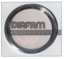
Figure 1.21. DIAFILM OP CVD diamond window
manufactured by De Beers Industrial Diamond (after Reference [80]).
One major potential market for CVD diamond is that of electronic devices. One limiting factor for current computer technology is how close components can be packed on a silicon chip. The closer the packing achieved the faster a chip can operate, however this leads to severe heat management problems. If electronic devices can be fabricated from CVD diamond the high thermal conductivity of the material would allow much closer packing of components, and therefore faster computers.
1.14. Low Temperature Growth of Diamond (LTGD)
One significant limitation of CVD growth of diamond
using 1%CH4/H2 gas mixtures is the requirement of the
substrate to be maintained at ~900°C. A major
goal in the field of diamond CVD is the lowering of substrate temperatures
required for growth, as this could permit the use of a much wider range of
substrate materials of industrial importance, such as aluminium, GaAs, nickel
and steel. It has been reported that
the use of both halogen [[81]]
and oxygen containing gas mixtures allows such growth at reduced Tsub
[[82]]. The following sections will discuss the
investigation of H/C/O containing gas mixtures for diamond CVD, focusing in
particular on CH4/CO2 feedstocks, and therefore serve as
an introduction to the results presented within Chapter 5.
1.14.1. H/C/O containing diamond CVD gas mixtures
Many gas mixtures containing varying ratios of O, C
and H have been investigated in the search for a viable low temperature diamond
deposition process. In 1991, Bachmann et al. [[83]] collated the results from over 70 such deposition experiments
to produce an atomic C-H-O phase diagram for diamond deposition (Figure 1.22),
showing that low pressure synthesis of good quality diamond is only possible
within a well defined area close to the H-CO tie line. This indicated that the exact nature of the
source gases is unimportant for most diamond CVD processes, and that it is only
the relative amounts of C, H and O which govern whether diamond deposition
takes place.

Figure 1.22. A simplied form of the Bachmann atomic C–H–O
diagram. Below the H‑CO tie‑line,
no growth is achieved. Above the H-CO
tie-line, non-diamond carbon is generally deposited, except in a narrow window
close to the tie-line, which produces polycrystalline diamond. Note that most experiments involving a few
per cent CH4 in H2 are constrained to a small region in the lower
left-hand corner (after Reference 16).
The diagram partitions into three distinct regions associated with: (a) diamond growth, entered on the H‑CO tie line where the input mole fractions of carbon and oxygen are equal (i.e. [C] = [O]); (b) no growth, lying below the H‑CO tie line (i.e. [C] < [O]); and (c) non-diamond growth, located above the H‑CO tie line (i.e. [C] > [O]). Experiments by Marinelli et al. [[84]], using a variety of hydrocarbon/CO2 gas mixtures, confirmed the presence of three such regions, and also refined the position of the boundaries between them.
Beckmann et al.. [[85]] investigated a limited number of cuts across the H‑CO tie line, using a model that considered just gas phase reactions, and concluded that oxygen regulated the concentration of reactive carbon species by reaction to form CO, thus accounting for the no-growth region for [C] < [O]. Ford [[86]] modelled the competition between diamond and non-diamond growth, and found the boundary between these two regions to correlate with the line ([C]‑[H])/[O]) = 0.07 in the Bachmann diagram (Figure 1.23).
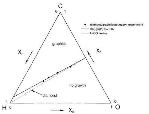
Figure 1.23. Phase
diagram for carbon film deposition, showing experimental points on the
diamond/graphite domain boundary [84], and a straight line fit corresponding to ([C]‑[H])/[O] = 0.07
(after Reference 86).
More recently, Eaton and Sunkara [[87]] used a CHEMKIN model that considered both gas phase and gas-surface chemistry to calculate mole fractions of C, H and O containing radical species, which were then plotted in the form of a ternary C-H-O diagram. It should be noted, however, that this study covered only a small section of the conventional Bachmann diagram.
1.14.2. CH4/CO2 Diamond CVD Gas Mixtures
The use of CO2/CH4 gas mixtures in microwave plasma CVD (MWCVD) has been reported to enable lower temperature growth [[88],[89]]. However, the process window for this gas mixture is very narrow and centred at a composition of 50%CH4/50%CO2 by volume flow rate [[90],[91]]. Such gas mixtures are unusual in that they contain no input hydrogen, compared to the excess used in other gas mixtures (although the concentration of H2 in the activated gas mixture is approximately half that seen in CH4/H2 mixtures). It has been proposed [[92]] that O, O2 and OH species in the plasma perform some of the roles of the H atoms, such as etching of non-diamond carbon [90] and the removal of unsaturated hydrocarbons in the gas phase [[93]]. However, no direct evidence has been presented to support these ideas.
To date, simple optical emission spectroscopy (OES) studies have been the major diagnostic applied to CO2/CH4 plasmas [90,91,[94]]. Balestrino et al. [94] found a correlation between optimum diamond growth rate (and quality) and the ratio of the emission intensities from CH (431 nm) and C2 (505-517 nm) species, and suggested this as a practical gauge to optimize growth conditions for unfamiliar gas mixtures. Mollart and Lewis [90] found that the ratio of the Ha (656 nm) and C2 emission peaks varied with gas composition, but that this ratio had only a weak correlation with the diamond deposition domain. OES studies in our own group [91,[95]], involving a wide range of gas mixing ratios (0-60% CH4), showed that maxima in the emission intensity ratios of CH:C2, H:C2 and CH:C3 could all be used as indicators for optimal diamond growth conditions. It was also found that at >55% CH4 the plasma produced significant amounts of soot, which caused a rising background in the emission spectra at longer wavelengths (>500 nm). This background was attributed to black body emission from soot particles in thermal equilibrium with the gases in the plasma region. Fitting this background curve to the Planck distribution function allowed an estimate (2000 K) of Tgas to be made.
1.15. Semiconducting CVD diamond for Electronics
As mentioned in Section 1.13, an area of great scientific interest is the fabrication of electronic devices based on semiconducting diamond. In order to obtain such material, atoms need to be introduced into the diamond lattice which modify the electronic band structure of the material, a process that is termed doping. Figure 1.24 presents a schematic diagram of the band structure of intrinsic (undoped), p- and n-type CVD diamond. It is clear that the large (5.4 eV) band gap of intrinsic CVD diamond (Fig.1.24(a)) makes promotion of electrons from the valence band into the conduction band impossible at room temperature (for illumination at wavelengths >200 nm). Therefore under such conditions diamond is an electrical insulator.
However, introducing atoms that have a lower atomic number than carbon into the diamond lattice produces acceptor levels within the band gap (Fig.1.24(b)). If this energy gap between the valence band and these acceptor levels is sufficiently small, electrons will be promoted into the acceptor levels, thus leading to conduction via holes within the conduction band (i.e. p‑type, indicating positive charge carriers). On the other hand, if atoms with a larger number of valence electrons than carbon are introduced, then donor levels are produced, which if of an energy sufficiently close to the conduction band (Fig.1.24(c)) provide electrons which can be promoted into this band leading to conduction (i.e. n-type, indicating negative charge carriers).
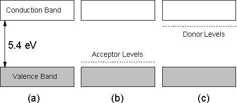
Figure 1.24. Schematic
diagram of the band structure of (a) undoped, (b) p-type and (c) n‑type
diamond.
Some electronic devices require both n- and p-type semiconducting diamond. As the following section will show, p-type material is readily obtainable but n-type CVD diamond has proved a much greater technical challenge. Devices that have already been fabricated from diamond include sensors intended for use in harsh environments (e.g. space, nuclear material reprocessing or particle accelerators) such as X-ray [[96]], radiation [[97]] and UV detectors [[98]]. Other applications make use of diamond’s extreme properties for use in telecommunications, for instance in the form of surface acoustic wave (SAW) devices [[99],[100]] (for possible use in mobile phones), or micro-relay switches [[101]] (for future use in high power microwave amplifiers). A major field of interest is the application of diamond as a cold cathode material in field emission displays (FEDs) [[102]]. Such devices aim to exploit the negative electron affinity of diamond whereby electrons may be emitted from this surface into vacuum with no barrier. If electrons can be supplied, diamond should emit electrons at very low applied fields [[103]].
1.16. p-Type CVD Diamond
It has been known for decades that natural boron‑containing (type IIb) diamonds exhibit p‑type semiconductor behaviour [[104]]. In the late 1970s, Derjaguin et al. reported the use of boron‑containing gas mixtures for the deposition of p-type diamond layers on diamond substrates [12]. Since then Fujimori et al. have carried out similar experiments utilising B2H6 additions to a MW activated 6%CH4/H2 gas mixture [[105]], thus leading to the routine use of MW and HFCVD methods for the growth of p-type diamond films by boron doping [[106],[107]].
1.16.1. H-induced p-type Surface Conductivity
In 1989 Landstrass and Ravi reported [[108]] that heat treatment of CVD diamond films increased the resistivity of the films by up to 6 orders of magnitude. As this increase was reversed by hydrogen plasma treatment it was concluded that the low resistivity of the as grown films was due to hydrogen passivation of deep traps within the film. Jackman et al. have shown that MWCVD deposited polycrystalline diamond films exhibit p-type surface conductivity due to a surface or near surface hydrogen layer [[109]].
Further insight has since been provided by Ristein et al. in work [[110]] which proved that this surface conductivity required not only a hydrogenated surface, but also such a surface in contact with air. This group proposed an electrochemical mechanism in which electron transfer occurs from the diamond to an absorbed molecular water layer (Figure 1.25). This results in a bending of the diamond valence band and the formation of a hole accumulation layer, leading to surface conductivity.
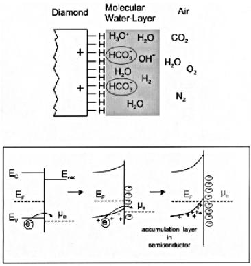
Figure 1.25. Top: Schematic
picture of the hydrogenated diamond surface in contact with a water layer as it
forms in air. Bottom: Evolution of band bending during the electron transfer
process at the interface between diamond and the water layer. After Reference 110.
1.17. Investigations of n-type CVD Diamond
As discussed in Section 1.16, CVD diamond films exhibiting p-type semiconductor properties are routinely grown by addition of B-containing gases to the standard CVD gas mixture (1%CH4/H2). However, obtaining n-type semiconducting diamond films by CVD has proved more challenging, mainly due to the fact that potential donor atoms (e.g. P, O and As) are larger than carbon, discouraging incorporation into the diamond lattice.
Nitrogen readily incorporates into diamond, however the resulting donor level is too deep (1.7 eV) [[111]] to be of any use for device applications. Several works have been published relating to phosphorus doping of CVD diamond [[112]-[115]], although these results have proved to be irreproducible. To date, the best results have been obtained by a group at NIRIM who reported the growth of n-type homoepitaxial diamond films, using PH3 additions (150‑3000ppm) to 0.15%CH4/H2 gas mixtures during MWCVD [[116]]. This result was recently reproduced by another group [[117]].
1.17.1. Sulfur Doping Experiments
n-Type conductivity has also been reported by the method of sulfur ion implantation into CVD homoepitaxial diamond (100) films [[118]]. Barber and Yarbrough [[119]] have shown that diamond growth is possible using mixtures of a few percent CS2 diluted in hydrogen, within a HFCVD reactor. Although no electronic measurements were conducted, their work has encouraged several subsequent investigations of H2S as another possible source of sulfur for in situ doping of CVD diamond films. Furthermore, Sakaguchi et al. [[120]-[122]] have reported that H2S addition to a 1%CH4/H2 gas mixture during MWCVD leads to the growth of semiconducting, homoepitaxial diamond films exhibiting n-type behaviour. Film growth rates were observed to decline with increased H2S addition, however, the quality of the films (as assessed via Raman spectroscopy) was found to be comparatively insensitive to changes in H2S addition. Relatively high Hall mobilities (597 cm2 V‑1 s‑1) were measured [120] for films produced using H2S doping levels of 50-100 ppm. Subsequent re-analysis of these samples [[123]] has raised some uncertainties with these results, however.
1.17.2. Ab Initio Calculations for Sulfur Related Defects
As Table 1.5 shows, ab initio calculations have given varying activation energies (i.e. level of donor level below conduction band) for the neutral sulfur defect (S0). One interesting observation is that co-doping CVD diamond with nitrogen or boron along with sulfur is predicted to give relatively low lying donor levels (e.g. S-N, S-B-S and either S2N2 or SN3 within a lattice vacancy). This gives an indication of a possible future route to n-type CVD diamond.
|
Defect |
Author |
Reported Activation Energy / eV |
Reference |
|
S0 |
T. Miyazaki et al.. |
1.2 (C3v) 1.1 (C2v) |
|
|
|
D. Saada et al.. |
0.15 |
|
|
|
T. Nashimatsu et al.. |
0.86 (Td) 1.63 (C3v) |
|
|
|
T. Albu et al.. |
1.93 |
|
|
S+ |
D. Saada et al.. |
0.50 |
125 |
|
S-B |
T. Albu et al.. |
1.49 |
127 |
|
S-N |
T. Miyazaki et al.. |
0.50 |
124 |
|
S-B-S |
T. Miyazaki et al.. |
0.50 |
124 |
|
V-S2N2 *) |
T. Miyazaki et al.. |
0.50 |
124 |
|
V-SN3 *) |
T. Miyazaki et al.. |
0.40 |
124 |
*) V denotes a vacancy in the diamond lattice.
Table 1.5. A review of ab
initio predictions for the activation energies of a variety of defects
within the diamond lattice (adapted from Reference [128]).
1.17.3. Gas Phase Studies of Sulfur Doping of CVD Diamond
Most of the work involving n-type doping of CVD diamond has focused on the electronic properties of the resultant films, rather than the gas phase chemistry leading to deposition. Dandy [[129]] presented simple thermodynamic equilibrium calculations for H2S/CH4/H2 gas mixtures (Figure 1.26), and concluded that the probable sulfur precursor dopant species was the SH radical, rather than the more stable species CS.

Figure
1.26. The effect of initial H2S concentration on the equilibrium
distribution of gas species at 115 torr and different temperatures (plotted in
K). Plots corresponding to two levels
of H2S addition to a 4%CH4/H2 gas mixture are
presented (after Reference 129).
In the work of Sternschulte et al. [[130]], gas was sampled via a glass capillary tube at a point downstream from the MW plasma, and was analysed by a quadrupole mass spectrometer. They showed that H2S addition to a 1%CH4/H2 MW plasma caused a decrease in CH3 concentrations leading to a decrease in diamond film growth rate, with the conclusion being that CH4 and H2S were reacting in the gas phase to form CS, as shown by Figure 1.27. This work also suggested that lowering Tsub may influence the growth of S-doped CVD diamond films.

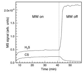
(a)
(b)
Figure 1.27. Plots of
species mass spectroscopic signal versus time for (a) CH4 and H2S
and (b) H2S and CS as measured by sampling gas through a capillary
placed below the level of the substrate holder in a MWCVD reactor (adapted from
Reference 130).
There is clearly scope for further investigations of sulfur containing diamond CVD gas mixtures, in order to gain a better understanding of the chemistry occurring in such systems. To this end, MBMS studies of H/C/S and H/C/O/S containing MW plasmas are presented within Chapters 6 and 7, respectively.