2. Film Analysis
2.1. Introduction
This section aims to introduce the techniques by which deposited diamond films were analysed. Further experimental details will be given in Chapter 3. The two methods of film characterisation most widely used were, scanning electron microscopy and laser Raman spectroscopy. A large proportion of films were also examined by X-ray photoelectron spectroscopy and four point probe electrical resistance measurement.
2.2. Scanning electron microscopy (SEM)
This method is commonly used to characterise diamond films, since inspection of SEM micrographs provides valuable information on the topology of the diamond films. Generally two views of the film are examined:
· Top View - gives an indication of the surface crystallinity (and therefore quality) of the diamond film.
· Cross-section - used to measure the thickness (and therefore growth rate) of the diamond film.
It should be noted that SEM does not provide unambiguous proof that a sample is diamond as only surface morphology is investigated.
A schematic diagram of an SEM apparatus is given below in Figure 2.1. A detailed description of the technique and background theory can be obtained from Reference [1], however a brief introduction will be given here. Electrons are produced via thermionic emission from an electron gun and focused down to a spot on the specimen by a system of ion optics (i.e. electromagnetic coils). A set of scan coils are used to scan (or raster) the spot over the surface of the sample and reflected electrons are collected, amplified and converted into a video signal. Thus, a micrograph of the specimen is obtained in the form of a 2-D plot of reflected electron intensity.
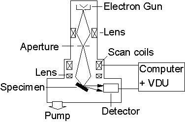
Figure 2.1. Schematic
diagram of a scanning electron microscope (adapted from Reference 1).
Electrons are normally accelerated to energies in the range of 0 to 30 keV and focused to a spot size of ~ 10 nm. The dimensions of surface features which can be resolved are essentially determined by this spot size. SEM analysis is a high vacuum technique requiring pressures of less than 10-6 Torr. In order to prevent electrical charging during analysis, the sample is first sputter coated with a conducting material (usually Ag or Pt).
2.3. Laser Raman Spectroscopy (LRS)
Raman spectroscopy is a powerful technique applicable to the investigation of materials in the gas, liquid or solid phases. The method finds widespread use as it is non-destructive and also requires no sample preparation. The Raman effect is an interaction between monochromatic light, usually a laser beam, and the chemical bonds within a specimen. When the laser beam interacts with the sample most of the light is scattered at the same wavelength (Rayleigh scattering) but a small proportion of the incident photons may excite molecular, or in the case of crystalline solids, lattice vibrations within the sample. These photons will be scattered with a slightly longer wavelength, due to the energy lost to the specimen. The difference in wavelength is referred to as the Stokes shift. Conversely, energy can also be imparted to the incident photon beam upon relaxation of the excited vibrations present in the sample, thus giving rise to anti-Stokes scattering, in which light is scattered at a slightly shorter wavelength from the specimen. Thus, LRS provides information on the types of bonding present within a sample, e.g. sp3 and/or sp2 hybridisation of carbon.
Figure 2.2 presents a schematic representation of a typical laser Raman spectrometer system. The laser beam is first collimated by a converging/diverging telescope before passing through a filter to remove any plasma emission lines. The beam is then focused into a spot (~50 mm) on the sample via an optical microscope, thus it is possible to control the area of sample to be examined. Scattered light is then collected and passed back into the spectrometer through a notch filter, which removes light at the laser wavelength. After passing through a slit (50 mm) the light is dispersed by a diffraction grating and then focused onto a cooled charged coupled device. A PC then handles subsequent data analysis and storage.

Figure 2.2. Schematic
diagram of a typical laser Raman apparatus (adapted from Reference [2]).
Here follows a discussion of the Raman spectra of CVD diamond films and other carbon materials under 514 nm laser excitation. A Raman spectrum of a single crystal diamond (i.e. sp3 bonding) is presented in Figure 2.3(a). A prominent first order peak is evident at 1332 cm-1, typically possessing a small full width at half maximum, FWHM, of ~ 2 cm-1.

Figure 2.3. LRS spectra of (a) single crystal
diamond, (b) graphite and (c) microcrystalline graphite (adapted from Reference
[3]).
Figure 2.3 also shows Raman spectra obtained from a sample of crystalline graphite (i.e. sp2 bonding) that exhibits a sharp peak at 1580 cm-1. The LRS spectrum of microcrystalline graphite (Fig. 2.3(c)) includes peaks at ~1355 and 1580 cm-1 which are due to disordered and graphitic phases [3], named the D and G bands, respectively . Amorphous carbon samples also give a similar Raman spectrum to this [[4]].
It is also clear from Figure 2.4(a) that the Raman spectram of CVD deposited diamond films can be more complicated than either that of graphite or single crystal diamond. In addition to the diamond peak at 1332 cm-1 there are also contributions from the D and G graphite peaks, caused by graphitic inclusions at the grain boundaries [[5]]. Both are broadened, with the former underlying the diamond peak, and the latter present as a wide band at ~ 1500 cm-1.
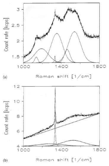
Figure 2.4. LRS spectra of two CVD deposited diamond
films. Each spectrum is shown along
with a fit obtained by addition of a number of Gaussian lineshapes. (a) is of low quality, as indicated by the
high degree of non-diamond components detected, whereas (b) exhibits little
contribution from these indicating high quality (adapted from Reference [6]).
LRS analysis of a sample deposited under different conditions is presented in Figure 2.4(b). This spectrum is clearly dominated by the diamond 1332 cm-1 line, with a small contribution from a severely broadened G band, indicating low non-diamond content. Such variations in film spectra with deposition conditions have led to the use of LRS for the determination of film quality, i.e. the diamond (sp3) versus non‑diamond (sp2) content. One simple qualitative measure of quality is the ratio of the diamond (1332 cm-1) to G band (~1550 cm-1) peak intensities, Id/IG [[7]]. As Figure 2.4 shows spectra can be analysed by curve fitting using linear baselines and Gaussian line-shapes, thus allowing calculation of Id/IG.
However, the sensitivity of the Raman technique not only varies with the wavelength of laser excitation (Reference [8]), but also changes between the different phases themselves. This is due to different phases having different Raman cross-sections. For instance, at the wavelength used throughout this thesis, 514 nm, LRS is ~50 times more sensitive to graphite [[9]], and ~233 times more sensitive to amorphous carbon [[10]], than to diamond. It should also be noted that there are additional contributions to the Raman spectra of CVD diamond films. For example, the spectrum given in Fig. 2.4(a) has been fitted using bands centred at 1140 and 1180 cm-1 (nanocrystalline diamond [7,[11]] or polyacetylene present in grain boundaries [[12]]) and 1460 cm-1 (polyacetylene [12] linked with bands at ~ 1160 cm-1 or a diamond precursor [6]).
Due to the difficulties caused by the presence in CVD diamond films of various carbon phases, all with differing Raman cross-sections, it has been proposed [10] that Raman spectra of such films should be analysed in terms of a quality factor, Q. This is defined in terms of the integrated area of the diamond line, Ad, and the combined integrated areas of all the non-diamond Raman bands. If it is assumed that these non-diamond components are all amorphous carbon, then Q can be defined as a percentage, as shown below:
![]() Equation
2.1
Equation
2.1
It should be concluded that, while it is possible to obtain an estimate of the quality of a CVD film by comparing the diamond and graphite peaks in its Raman spectrum, the complete deconvolution of spectra to provide quantitative measurements (e.g. of sp3/sp2 ratio) is generally not possible.
2.4. X-ray photoelectron spectroscopy (XPS)
A
detailed description of X-Ray Photoelectron Spectroscopy is given in Reference 1, however a brief introduction will be given here. XPS
is a technique used to investigate the composition of deposited films by
ionizing surface atoms and measuring the energy of ejected photoelectrons. The method requires the sample of interest
to be bombarded with low energy X-rays, produced from an aluminum or magnesium
source, with an energy of hv.
These X-rays cause electrons to be ejected from either a valence or
inner core electron shell. The energy
of the electron, E, is given by E = hv - E1 - Ф,
where E1 is the binding energy of the atom and Ф is the
work function of the sample. Thus, it
is possible to calculate the binding energy of the ejected electron, and
therefore identify the atom (and its chemical state) from which the electron
originates. In order to prevent surface
contamination, analysis is carried out under ultra high vacuum (< 10-10
Torr).
As
Figure 2.5 illustrates, X-rays are directed onto the sample and the resulting
photoelectrons are then focused onto the entrance slit of a concentric
hemispherical analyzer. Here a negative
and positive potential are applied to the outer and inner cylinders,
respectively, such that the central line between the cylinders is a line of
zero potential. Scanning the potentials
allows control of the energy of electrons that are allowed to pass through the
analyzer and onto the detector, usually a channel electron multiplier
(channeltron).
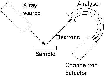
Figure
2.5. Schematic diagram of XPS apparatus.
One major disadvantage is the low spatial resolution of the technique, in most cases the analysed area is required to be of the order of a few square mm. Another problem is that only the surface of a sample can be analysed, thus little information relating to the bulk is obtained. This problem can be minimised by carrying out depth profiles in which a beam of argon ions is used to etch away the surface between XPS analyses. In such a way the bulk of a sample can be investigated with XPS.
By the comparison of different XPS peaks it is possible to obtain qualitative measurements of relative elemental compositions for materials using XPS. Further details of this analysis will be given in section 3.3.3.
2.5. Four point probe resistance measurements
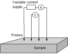
The four-point probe method is used to measure the electrical resistance of deposited films. This technique forces a fixed current through the sample, using two outer probes (See figure 2.6), and measures the resulting voltage between the two inner probes. The advantage of such an arrangement over two probe experiments is that the effect of any contact resistance between the sample and probes is cancelled out. As a result of the electrical contacts being made to the surface of the film, such measurements are prone to give results more representative of the surface, rather than the bulk of the sample. This is a particular problem when this technique is applied to polycrystalline CVD films as the surface electrical conduction is controlled by factors, such as grain boundary content and surface termination, which can vary from film to film. However this technique does give an impression of how the electronic properties of films change with deposition conditions.
Figure
2.6. Diagram of Four-point probe resistance measurement.