Chapter 3
Electrical Contacts
3.0 Outline
·
This
chapter describes the electrical contacts between the diamond electrodes and
the copper connecting wires.
·
The
requirement for Ohmic contacts is discussed. A schematic illustration of the
energy levels at the interface between a p-type semiconductor and a metal is used to illustrate a
Schottky barrier.
·
Details
are given for the fabrication processes for two types of Ohmic contact: three
layer metal contacts and titanium underlayer contacts. The practicality of the
two processes for use in the laboratory is compared.
·
Current-voltage
plots are presented for the four types of contacts described in chapter 2.
Silver epoxy resin contacts are considered to be sufficient for highly doped
diamond samples when used over a small voltage range. For low doped samples,
titanium underlayer contacts give the best performance.
3.1 Introduction
As the low doped diamond
films exhibited semiconducting behaviour, it was necessary to study the
metal-diamond contacts to ensure that they obeyed Ohm’s law. For highly doped
diamond films, satisfactory contacts could be fabricated by using silver dag to
attach copper wires to the diamond surface. However, this simple technique was
not possible for low doped films, as Schottky barriers would form at the
semiconductor-metal interface. Figure 3.1 shows a schematic energy diagram of a
Schottky barrier.
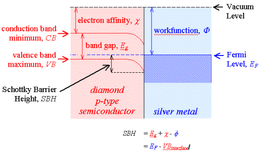
Figure 3.1 - The
Metal-Semiconductor Interface
The properties of two types
of contact were studied: three layer metalisation (3LM) and titanium
underlayers (TiUL).
Ohmic contacts are defined
as metal-semiconductor contacts that have negligible contact resistance to the
bulk or series resistance of the semiconductor. A satisfactory Ohmic contact
should not significantly degrade device performance and pass the required
current with a voltage drop that is small compared with the drop across the
active region of the device. 113
The simplest techniques used
to reduce the Schottky barrier height involve the use of diamond with a
hydrogen terminated surface (to decrease c) and electronegative metals
(to increase f). 101 Silver dag
contacts were easy to fabricate but gave poor results, as shown in figure 3.3.
Evaporating gold onto the surface of diamond gave inconsistent results as the
gold layers readily delaminated.
Titanium has been used to
fabricate low-resistance contacts 72,114-116 and it has been shown
that annealing at temperatures greater than 400 °C leads to the formation of a
titanium carbide layer at the interface. 114
The reactivity of titanium
posed a practical problem as the metal had a tendency to oxidise.
3.2 Fabrication of Three
Layer Metal Contacts
An overview of the design of
the three layer metal (3LM) contacts is presented in section 2.9.3.
To prepare the sample for
titanium deposition, a pre-treatment was required to oxidise the surface and
remove hydrogen and non-diamond carbon from the surface. To achieve this, the
film as exposed to chromic acid at 95 °C for a period of about two hours.
The diamond samples were
then loaded into the evaporator. It was necessary to heat the sample to remove
physisorbed species from the diamond surface prior to titanium deposition to
prevent oxidation of the metal. The samples were placed on a heating stage
inside the vacuum chamber of the evaporator. A mask was then placed over the
sample and a tungsten basket (Alfa Aesar) positioned above the mask and loaded
with titanium crystals (Alfa Aesar). The bell jar was placed over the assembly
and the system was pumped down to less than 2 ´ 10-5 Torr. The sample was
then heated to 200 - 250 °C.
The masks were made from 0.5
mm thick mild steel foil and contained circular holes (diameter = 2 mm, spacing
= 8 mm).
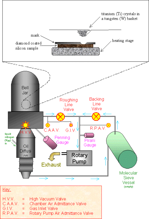
Figure 3.2 - A schematic diagram of the evaporator
An alternating current was
passed through the tungsten basket to evaporate the titanium. A layer of
between 100 - 150 nm of titanium was deposited at a rate of approximately 0.4
nm/min as monitored by using a quartz crystal microbalance.
After the titanium
deposition, the sample was allowed cool slowly under vacuum and it was often
left overnight to reach room temperature. The cooling time could have been
substantially reduced by flowing a dry oxygen-free gas through the chamber but
cooling in vacuum proved sufficient for these studies.
To obtain the required depth
of titanium (100 - 150 nm), it was sometimes necessary to repeat the loading,
heating, deposition and cooling process with a second load of titanium
crystals.
The sample was then
transferred to a sputter coater and a 40 nm thick platinum spot was sputtered
over the titanium. A mask was used with a 3 mm diameter spot (a diameter greater
than that used for the titanium deposition). This ensured complete coverage of
the titanium by platinum.
The sample was then returned
to the evaporator and a gold spot with a depth of approximately 100 nm was
deposited over the platinum. A spot with a diameter of 4 mm was used to ensure
complete coverage of the platinum.
After each step of the
process, the three layer metal structure could be examined by eye and with an
optical microscope to check the alignment, coverage and quality of the metal
layers.
The final step of the
process was to anneal the sample. A survey of the literature suggested that an
anneal in vacuum at a temperature of 500 °C would be sufficient to allow the
titanium carbide layer to form. 114,117 This was achieved by a two
stage heating process. The first stage provided the necessary vacuum and the
second stage reached the necessary annealing temperature. The samples were
loaded in a quartz cell, designed with two taps to allow the contents to be
pumped down to vacuum with a rotary pump and then flushed with oxygen-free
nitrogen (N2) or helium (He) (BOC Speciality Gases). The vessel
was then routinely
flushed several times with nitrogen to remove oxygen before a cement oven was
used to heat the cell to 200-250 °C. This heating was performed while the cell
was being continuously evacuated by a rotary pump. This removed species as they
desorbed from the sample and the walls of the vessel. While still being heated,
the cell was sealed and it was then transferred to a high temperature furnace
for annealing at 500 °C.
A number of anneals were
performed under a static atmosphere of helium to investigate the effect on the
sub-surface hydrogen in the films. †
These helium experiments did not yield useful results.
The fabrication process for the
3LM contacts is summarised in table 3.1 and the electrical characteristics are
described in section 3.5.
The Ti/Pt/Au metallization scheme represents the
simplest of a range of titanium based metallurgical systems. Other proposed
schemes include the Ti/W/W(Ni3Sn4)/Ni3Sn4/Au
scheme proposed by Katz et al. 118
The fabrication process for
the 3LM contacts had a number of drawbacks:
·
The
complicated design required a large number of steps which increased variation
between samples and the likelihood of flaws.
·
A
hot acid pre-treatment was required which prevented study of hydrogen
terminated diamond. However, the process could, in principle, be modified by
designing a cell to expose only a selected area of diamond to the acid.
·
The
process was time consuming. A minimum of six working days were required to grow
the film but restricted availability of the platinum sputter coater and the
high temperature furnace resulted in practical lead times of over a fortnight.
·
Despite
modifications to reduce the effects of vibrations in the evaporator, the
alignment of the three concentric circles was not always sufficiently accurate.
The sample had to be heated to form the carbide
layer which led to oxidation of the titanium and possible changes to the
diamond surface.
Step |
Description |
|
1 |
abrasion
of the silicon substrate abrade with diamond powder to provide nucleation
sites |
|
2 |
cleaning substrate to remove excess diamond powder (a)
wipe with IPA soaked cotton buds (b)
place in a beaker of IPA in an ultrasonic bath |
|
3 |
diamond deposition (a)
load substrate into chamber (b)
evacuate chamber (c)
pre-heat substrate (d)
deposit diamond for several hours (e)
initially cool in a hydrogen atmosphere (f)
cool to room temperature in vacuum |
|
4 |
surface pretreatment (a)
heat sample in chromic acid (b)
rinse sample with ultrapure water |
|
5 |
titanium deposition (a)
load substrate into evaporator (b)
align mask over sample (c)
evacuate chamber (d)
heat sample to remove physisorbed species (e)
evaporate titanium on to diamond surface (f)
cool sample to room temperature in vacuum (g)
repeat of steps (c) to (f) with more titanium |
|
6 |
platinum deposition (a)
load substrate into evaporator (b)
align mask over sample (c)
evacuate chamber (d)
sputter platinum over titanium spot |
|
7 |
gold deposition (a)
load substrate into evaporator (b)
align mask over sample (c)
heat sample to remove physisorbed species (d)
evaporate gold over platinum spot (e)
cool sample to room temperature in vacuum |
|
8 |
annealing (a)
place sample into quartz cell (b)
evacuate cell (c)
flush cell with nitrogen (d)
repeat (b) and (c) several times (e)
evacuate cell (f)
heat sample to 200 - 250 °C (g)
seal vessel and transfer to high temperature annealing furnace (h)
high temperature anneal at 500 °C (i)
cool to room temperature in vacuum |
|
9 |
attachment of wires (a)
attach copper wire with silver dag and allow to dry (b)
cover silver dag with epoxy resin to protect contact |
Table 3.1 - Summary of
the fabrication procedure for 3LM contacts
3.3 Fabrication of Titanium
Underlayer Contacts
The drawbacks of the 3LM
contact design led to the development of a simpler design, the TiUL contact. An overview of the design of
the titanium underlayer (TiUL)
contacts is presented in section 2.9.4.
The advantages of the TiUL contacts are detailed below:
·
A
reduction in the number of processing steps increased the reliability of the
finished device and reduced the time required processing time.
·
As
the diamond film was grown over the titanium, a carbide layer formed without
the need for annealing or any other post-treatments. Electrochemistry could
therefore be performed on an as grown surface and the titanium was much less
likely to be oxidised.
·
Platinum
and gold layers were no longer required.
·
A
single strip of titanium was applied directly to the silicon substrate and this
proved easier to fabricate that the concentric circles because the geometry was
simpler and the acceptable tolerances greater.
The only disadvantage of the
TiUL contacts was the need to protect
the metal if any harsh post-treatments that were applied to the diamond sample,
such as acid dips. However, this drawback could be avoided by designing a cell
to selectively expose only the diamond surface to the treatment. The PTFE
electrochemistry cells, described in a later chapter, proved to be adequate for
the treatments used in this study.
The fabrication process for
the TiUL contacts is summarised in
table 3.2 and the electrical characteristics are described in section 3.6.
Step |
Description |
|
1 |
abrasion
of the silicon substrate abrade with diamond powder to provide nucleation
sites for subsequent diamond growth, leaving a strip of smooth silicon |
|
2 |
cleaning substrate to remove excess diamond powder (a)
wipe with IPA soaked cotton buds, working away from the smooth end (b)
clamp the substrate in an ultrasonic bath so that the abraded area is
dipped into IPA (c)
rinse sample with IPA flowing away from smooth end |
|
3 |
titanium deposition (a)
load substrate into evaporator (b)
align mask over the surface of the sample, leaving the smooth area
and part of the abraded area exposed. (c)
evacuate chamber (d)
heat sample to remove physisorbed species (e)
evaporate titanium on to diamond surface (f)
cool sample to room temperature in vacuum (g)
repeat of steps (c) to (f) with more titanium |
|
4 |
diamond deposition (a)
load substrate into chamber (b)
evacuate chamber (c)
pre-heat substrate (d)
deposit diamond for several hours (e)
initially cool in a hydrogen atmosphere (f)
cool to room temperature in vacuum |
|
5 |
attachment of wires (a)
attach copper wire with silver dag and allow to dry (b)
cover silver dag with epoxy resin to protect contact |
Table 3.2 - Summary of the
fabrication procedure for TiUL
contacts
3.4 Characteristics of
Silver Epoxy Resin Contacts
Silver dag contacts were
considered adequate for highly doped films (those grown with a boron to carbon
ratio of more than 3000 p.p.m. in the gas phase) when used over a narrow
potential range.
Figure 3.3 shows a
current-voltage plot for a diamond sample with a doping level of 3000 p.p.m.
Two silver dag contacts were applied to the top of the as-grown sample and the
scan was taken with a m-Autolab potentiostat (Eco Chemie B.V.) in a two electrode
configuration with a scan rate of 50 mV/s. The plot was asymmetrical over the
ten volt range of the scan. However, over a reduced range of - 0.5 V to 0.5 V,
the plot was linear (see inset). The reciprocal of the gradient was 475 W.
Figure 3.4 shows a similar
plot for a low doped sample. The diamond film was only doped by the residual
boron that contaminated the chamber after a growth run with an active doping
level of 3000 p.p.m. The graph is significantly less symmetrical than that for
the more highly doped sample and the curve is non-linear even near the origin
(see inset). Figure 3.5 shows the two graphs superimposed on the same axes. The
residually doped film was, as expected, more electrically resistive than the
actively doped film.
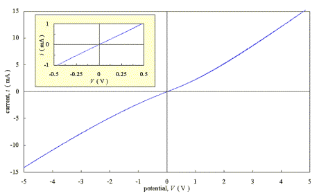
Figure 3.3 - Current-Voltage characteristics for an as-grown moderately doped diamond film with two silver dag contacts [sample B111]
![]()
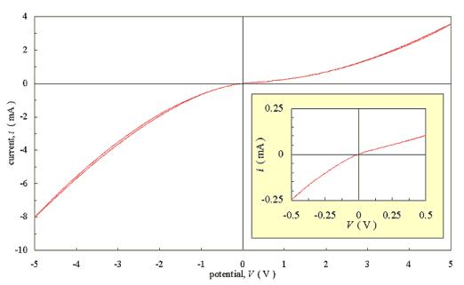
Figure 3.4 - Current-Voltage characteristics for an as-grown low doped diamond film with two silver dag contacts [sample B112]
![]()
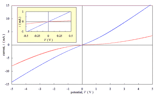
Figure 3.5 - Current-Voltage
characteristics for diamond films with two silver dag contacts [sample B111
& B112]
3.5 Characteristics of
Evaporated Gold Contacts
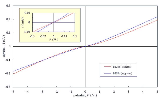
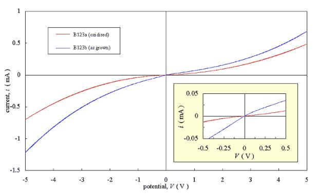
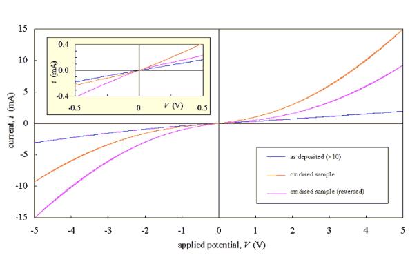
Figures 3.6 and 3.7 show current-voltage plots for two pairs of diamond samples. Each pair was grown in a single deposition run to minimise variation between the films. One sample from each pair was refluxed in chromic acid to oxidise the surface of the film; while the other sample from the pair was tested “as grown”. Two gold strips were evaporated onto each sample and current-voltage plots were measured. The gold layers had a thickness in the order of 100 nm.
Samples B128a and B128b were
grown with a gas phase boron to carbon ratio of 50 p.p.m.
Samples B123a and B123b were
only doped by the residual boron contamination in the CVD chamber.
The results showed
asymmetrical non-linear behaviour. The actively doped samples (B128a and B128b)
gave an approximately Ohmic response over a reduced potential range (-0.5 V -
0.5 V) while the residually doped samples (B123a and B123b) gave a non-linear
response.
It was believed that the
exposure to boiling chromic acid had successfully altered the hydrogen
termination of the diamond surfaces. A simple test with ultrapure water showed
the “as grown” samples to be hydrophobic and the oxidised samples to be hydrophilic.
Figure 3.7 shows an
increased resistance for the oxidised film. This agrees with theory outlined in
section 3.1 but the effect of surface termination on the contact properties
could not conclusively determined due to the lack of reproducibility of these
results.
Evaporated gold contacts did
not provide a significant improvement in performance over the simpler silver
dag contacts. The lack of adhesion between the gold and diamond may have been
responsible for this poor performance.