Chapter 4
Standard Electrochemical Theory
4.0 Outline
·
This
chapter outlines the standard electrochemical theory on which this study was
based.
·
A
comparison is made between the behaviour of metal and semiconductor electrodes.
·
An
expression is derived relating the steady state current to the overpotential
for surface state mediated charge transfer.
4.1 Metal Electrochemistry
In this section the
Marcus-Gerischer theory for electron transfer at a metal electrode is outlined.
Reference 119(a) contains details of the theory and lists the original
references and review articles.
Underlying this approach is the idea that electron transfer occurs
between occupied and unoccupied states that are equal in energy. 120
The total current density, j, at a metal-solution interface is the
sum of the anodic current density, ja,
and the cathodic density, jc.
By convention, the cathodic current is negative.
j = ja
+ jc . (equation
4.1)
Anodic current flows when
oxidation occurs at the electrode surface:
R → O + e- (e.g. Fe2+(aq)
→ Fe3+(aq) + e-)
Cathodic current flows when
reduction occurs at the electrode surface:
O + e-→ R (e.g. Fe3+(aq)
+ e- → Fe2+(aq))
In the Marcus-Gerischer
approach to electron transfer it is assumed that the Born-Oppenheimer approximation
applies, i.e., the nuclei, being so much heavier than the electron, move
relatively slowly and may be treated as stationary during electron transfer.
121 Hence electrons are transferred to energy levels at or near the Fermi
level in the metal. At a metal
electrode a change in the applied potential results in charging of the metal
which leads to a change in the potential at the surface. As the energy of the surface electrons is
altered the position of the Fermi level changes. However, the occupation of states about the Fermi level remains
constant. As a result the current
densities are simply proportional to the overlap integral of the Fermi function
in the metal and the density of states function for the solution species:
ja µ (overlap of EF and ER)
jc µ - (overlap of EF and EO)
Figure 4.2 shows a schematic
energy diagram for a metal-solution interface.
At the equilibrium
potential, the overlap integrals are equal. The values of ja and jc
are therefore equal and opposite and the net current density is zero. This
situation is shown to the left in figure 4.2.
At a positive overpotential,
the overlap integral for the reduced species is greater than that for the
oxidised species. The net current density is therefore positive. An anodic
current flows and oxidation of the reduced species occurs. This situation is
shown in the upper right diagram in figure 4.2.
At a negative overpotential, the overlap integral for the oxidised species is greater than that for the reduced species. The net current density is therefore negative. A cathodic current flows and reduction of the oxidised species occurs. This situation is shown in the lower right diagram in figure 4.2.
Figure 4.1 shows a sketch of
current density – overpotential relationship for the case where the transfer
coefficient, a = ½.
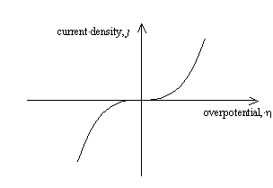
Figure 4.1 – current density as a function of overpotential for a metal
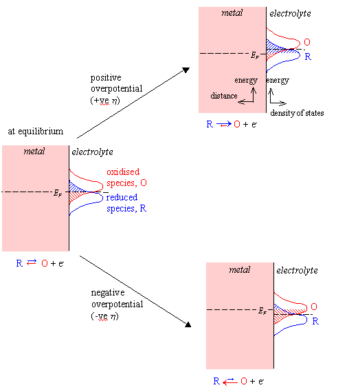
Figure 4.2 – Schematic Energy Diagram for a Metal-Solution Interface
4.2 Normal p-type Semiconductor
Electrochemistry
As for a metal electrode,
the total current density, j, is the
sum of the anodic and cathodic current densities (ja & jc).
The majority charge carriers in a p-type semiconductor are positive holes in
the valence band.
The anodic reaction:
R
+ h+(VB) → O (e.g.
Fe2+(aq) + h+(VB) → Fe3+(aq))
The cathodic reaction:
O
→ R + h+(VB) (e.g.
Fe3+(aq) → Fe2+(aq) + h+(VB))
The Born-Oppenheimer
approximation still applies but unlike the case for a metal electrode, charge
transfer can not occur at the Fermi level if the density of states is zero at
that energy (i.e. it is in the band gap of the semiconductor). Charge transfer
will occur at the surface energy of the valence band, EVB,S.
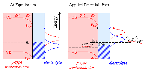
Current flow at a semiconductor electrode is dependent of the surface concentration of majority charge carriers. For a p-type semiconductor, the concentration of holes at surface is a significant factor in the rate of charge flow in the anodic reaction:
ja
µ (overlap
of EVB,S and ER) ´ ( [h+]surface )
Whilst for the cathodic
reaction the availability of electrons in the valence band is essentially
constant:
jc
µ - (overlap of EVB,S and EO)
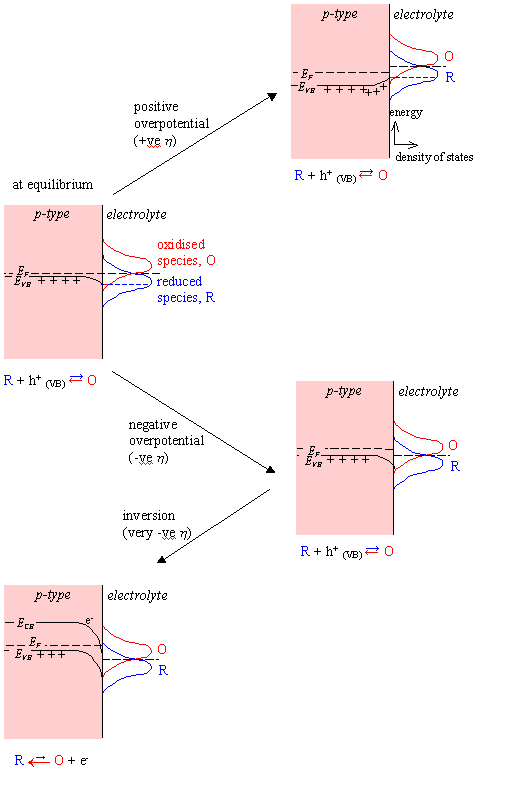
Figure 4.3 – Schematic Energy Diagram for a Semiconductor-Solution Interface
The overlap terms at the valence band edge are not affected by changes in potential. The cathodic current density will therefore remain constant.
jc = jc,0
At a positive overpotential, there will be a higher surface concentration of holes than at equilibrium. There is an exponential relationship between the concentration of holes and the overpotential. Therefore, at positive overpotential, the anodic current density will be greater than at equilibrium.
ja > ja,0
At negative overpotential,
the concentration of holes at the surface will be reduced and as the magnitude
of the negative overpotential is increased, the concentration will tend to
zero. The anodic current density, ja,
will therefore fall from its equilibrium value, ja,0.
The total current density, j, is the sum of the constant cathodic
current density, jc, and the variable anodic current density, ja. At increasing positive
overpotential, the total current density will rise rapidly, while at decreasing
negative overpotential, the total current density will fall to a constant
minimum value, equal to the equilibrium cathodic current density, jc,0.
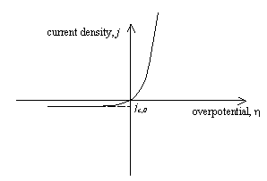
Figure 4.4 – current density as a function of overpotential for a semiconductor
At sufficiently negative
potentials, inversion can occur. This phenomenon occurs when band bending at
the surface of the semiconductor is sufficiently great that the Fermi level
lies in the conduction band. There will then be a finite probability of finding
a conduction band electron at the surface of the semiconductor. An anodic
current can flow and the total current density will be reduced in magnitude
( jc,0 < j < 0 ).
Anodic current flow due to
inversion:
O
+ e-(CB)→ R (e.g.
Fe3+(aq) + e-→ Fe2+(aq))
4.3 Highly doped
semiconductors
At high doping levels, the semiconductor becomes degenerately doped. The Fermi Level of the semiconductor lies within the valence band (VB) and the space charge region becomes very small. Electrons are able to tunnel from the bulk VB directly into the electrolyte. Therefore, the concentration of available charge carriers is constant and the electrode behaves like a metal.
ja µ (overlap of EF and ER)
jc µ - (overlap of EF and EO)
Cyclic voltammograms will
therefore show both oxidation and reduction peaks.
Figure 4.5 shows a schematic
energy diagram for a highly doped semiconductor-solution interface.
Figure 4.6 shows a sketch of
current density – overpotential relationship.
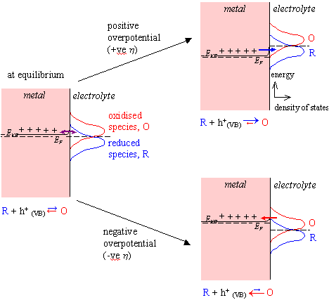
Figure 4.5 – Schematic Energy Diagram for a Heavily Doped Semiconductor-Solution Interface
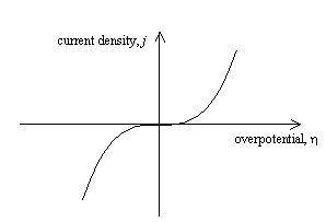
Figure 4.6 – current density as a function of overpotential for a heavily doped semiconductor
4.4 Surface State Mediated
Electrode Transfer
Electron transfer via surface states, see figure 4.7, is often invoked to explain anomalies in semiconductor electrochemistry. 122(a)
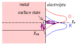
Figure 4.7 – electron transfer via a surface state
In the literature the development of a theory for this mechanism of charge transfer has been almost totally neglected. The exceptions are the works of Chazalviel and Vanmaekelbergh 123-124 where surface state mediated charge transfer at n-type semiconductors are considered. In this section the equations that govern the steady-state current at a p-type semiconductor electrode at which electron transfer occurs via surface states are developed. The theory is based on Marcus-Gerischer model. To facilitate the development of the theory a number of assumptions were made these are detailed below.
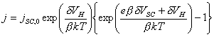
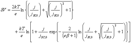
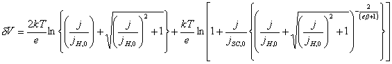
4.4.1 Contributions to the Applied Potential
The change in applied
potential across the electrode-solution interface, dV, has two contributions: the
potential difference across the space charge region in the solid, dVSC, and the potential
difference across the Helmholtz layer in the solution, dVH.
dV = dVSC + dVH (equation 4.2)
As shown in chapter 3, care
was required to ensure that electrical contacts to the electrode provided an
Ohmic response and did not contribute to the measured potential.
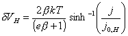
4.4.2 Contributions of the
Helmholtz Layer and the Space Charge Region
The capacitance of the
Helmholtz layer, CH, is
significantly greater than that of the space charge region, CSC. This implies that
changes to the potential drop across the Helmholtz layer, dVH, are only due to changes in the surface charge, dQ.
CSC << CH
![]()
(equation
4.3)
4.4.3 Electrical Charge at the Surface of a Semiconductor Electrode
The change in the surface charge is dependent on the
change in the Fermi level at the surface, E0,
and the density of states at the surface, rss.
![]()
(equation
4.4)
![]()
(equation
4.5)
If the distribution of surface states is uniform,
then the equation becomes:
![]()
(equation
4.6)
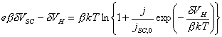
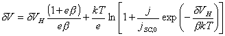
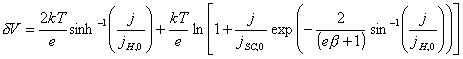
4.4.4 The Butler-Volmer Equation
Electron transfer across the
Helmholtz layer is governed by the Butler-Volmer equation. 120
Under non-equilibrium
conditions, there will be a difference in energy between electrons in the
surface states and the redox couple. The Butler-Volmer equation relates the current
density to the overpotential, h.
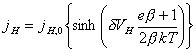
Assuming efficient mass transport:
![]() (equation
4.7)
(equation
4.7)
If a = ½,
![]() (equation 4.8)
(equation 4.8)
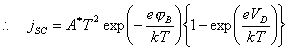
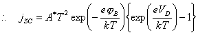
4.4.5 Schottky Diode
The bulk semiconductor - surface state junction may
be modelled as a Schottky diode. 125
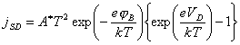
(equation
4.9)
where jSD = forward biased current
VD = the
potential drop between the space charge and the bulk semiconductor (the forward
bias)
jB = barrier height
A* = the “effective Richardson constant” (units of
A K‑2 cm‑2)
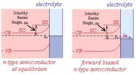
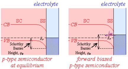
Figure 4.8 shows the
relationship between forward bias and conventional electrochemical current for
n-type and p-type semiconductors.