Chapter 7
Theoretical Model for the Electrochemistry of Boron Doped Diamond
7.0 Outline
·
This
chapter develops a theoretical model for the electrochemistry of boron doped
diamond.
·
The
relationship between current density and applied potential is investigated
·
The
AC impedance results are considered in terms of the surface state model.
7.1 Interpreting the
Metallic Behaviour of Highly Doped Diamond
Chapter 5 showed that highly
doped diamond films, with boron concentrations over 1020 cm-3,
exhibited metallic behaviour. Cyclic voltammograms of well known redox couples
showed both oxidation and reduction peaks.
Two possible explanations
for this behaviour are that:
·
The
samples are degenerately doped (see section 4.3).
·
Contamination
of the specimens provided a conduction path through the films. Feasible sources
of contamination include tantalum (Ta) from the filaments in the CVD reactor
and graphite (C) formed during diamond deposition.
These explanations can be
discounted because:
·
A
Mott-Schottky regime was observed, as shown in section 5.7 (figure 5.17).
·
Two
time constants were observed in impedance measurements of the films, as shown
in sections 5.8 – 5.9 (figures 5.24 – 5.25).
This implies that the electrode was a p-type semiconductor and the electron transfer occurred via a surface state.
7.2 Explanation of the Metallic Behaviour of Highly Doped Diamond
To explain the behaviour of boron doped diamond, the positions of the conduction band maximum, the valence band minimum and the Fermi level relative to the energy levels of the redox species in solution need to be considered.
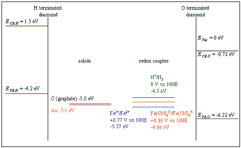
Figure 7.1 – Schematic energy level diagram showing the band edges of the semiconductor and the energy levels of redox species. Redox potentials from reference 12.
Figure 7.1 gives a schematic representation of the relevant energy levels. The band edges have been calculated from the work function of the semiconductor, assuming that there was no voltage drop across the space charge layer. 119(b)
7.2.1 Hydrogen Terminated Diamond
For hydrogen terminated diamond, the valence band maximum lies at a higher energy than the proton redox couple. Therefore, in aqueous solution, holes will accumulate at the surface.
A surface charge on the semiconductor and potential drop across the Helmholtz layer will result in the material behaving in a metallic manner.
Figure 7.2 provides a schematic diagram of the contact process using the standard hydrogen reaction as an example.
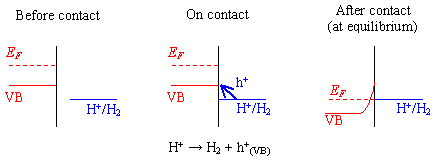
Figure 7.2 - Reaction at a Hydrogen Terminated Surface
7.2.2 Oxygen Terminated Diamond
The diamond samples, being polycrystalline in nature, contained a high density of grain boundaries. Grain boundaries are known to provide trapping states. 119(c) The grain boundaries in CVD diamond can be considered to be graphitic in nature. Therefore, the energy of the grain boundary states will be approximately –5.0 eV (the energy level of graphite). This energy level is comparable to the energy levels of the redox couples in aqueous solution.
Figure 7.3 provides a schematic diagram of the contact process for an oxygen terminated surface which involves the surface states. The diagram shows the case where the potential drop across the Helmholtz layer is constant. When this is not the case, any change in the potential across the Helmholtz layer would lower the level of the redox couple in solution relative to the valence band maximum.
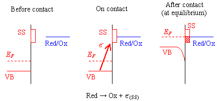
Figure 7.3 - Reaction at an Oxygen Terminated Surface (SS = surface state)
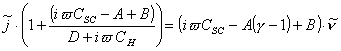
7.3 The relationship between current density
and applied potential
The model for surface state mediated electron transfer presented in Chapter 4 assumed that the potential drop over the Helmholtz layer was insignificant (§ 4.4.1). If this assumption is not valid, then the system may be modelled as shown in figure 7.4.
The Helmholtz region and the space charge region can be considered to be connected in series. Each region acts as a resistor in parallel with a capacitor.
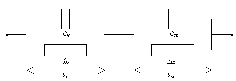
Figure 7.4 – Equivalent
circuit for surface mediated transfer with significant potential drop across
the Helmholtz region
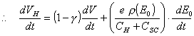
Applying Kirchhoff’s first law:
![]() (equation
7.1)
(equation
7.1)
![]() (equation
7.2)
(equation
7.2)
Using equation 7.2 to eliminate dVsc from equation 7.1:
![]() (equation 7.3)
(equation 7.3)
Qss = charge on the surface
states.
Let r(E0) be the density of states
per unit energy (eV):
![]() (equation
7.4)
(equation
7.4)
Hence:
 (equation
7.5)
(equation
7.5)
or ![]() (equation
7.6)
(equation
7.6)
where 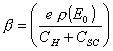 . (equation
7.7)
. (equation
7.7)
Assuming that the capacitances,
CH and CSC, and the density of
states, r(E0), are independent of the potential:
![]() (equation
7.8)
(equation
7.8)
and ![]() (equation
7.9)
(equation
7.9)
Substituting equation 7.9
into equation 4.8 (the Butler-Volmer equation for
a = ½):
![]()
![]() (equation
7.10)
(equation
7.10)
 (equation 7.11)
The current across the space
charge region, jSC can be
modelled as a Schottky diode (substitute equation 7.9) into equation 4.18:
![]() (equation
7.12)
(equation
7.12)
Combining equations 7.11 and
5.12 above, gives an expression for the total current, j, that varies with the overpotential, dV, and the currents across the space charge and Helmholtz regions,
jSC and jH.
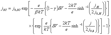 (equation 7.13)
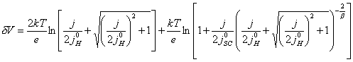
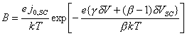
At steady state, the stored charge will be constant and the current through the Helmholtz layer must equal that through the space charge region.
j = jH = jSC (equation 7.14)
Therefore, equation 7.13 can be rewritten:
 (equation 7.15)
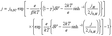
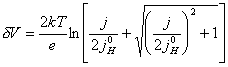
Equation 7.15 is an
expression for the current density, j,
that varies with the applied overpotential, dV. All the other terms are
constant. An analytical solution to the equation can not be obtained and so
numerical methods are necessary.
Mathcad 8 Professional (MathSoft, Inc.) was used to find numerical solutions. The software automatically selected an appropriate algorithm to solve a given equation. Non-linear solutions are found using the Levenberg-Marquardt, Quasi-Newton and Conjugate Gradient algorithms. The solutions found by numerical means were not necessarily unique. 139-142
As stated in section 4.4.2, it is usual in semiconductor electrochemistry to assume that the capacitance of the Helmholtz layer to be much greater than that of the space charge region (CH >> CSC). If this is the case, then g tends to unity (g ® 1) and the equation can be solved analytically.
When g = 1, then equation 7.15 simplifies to equation 7.16.
(equation
7.16)
7.3.1 Special cases of the current density -
applied potential relationship
7.3.1.1 The case where |j0H| >> |j|
For the case where |j0H| >> |j|, then several terms in
equation 7.16 become negligible. This leads to the much simpler relationship
given in equation 7.17.
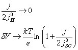 (equation
7.17)
(equation
7.17)
Figure 7.5 shows a Mathcad plot of equation 7.16 for the case where |j0H| >> |j|. The behaviour is independent of b and is typical of a p-type semiconductor.
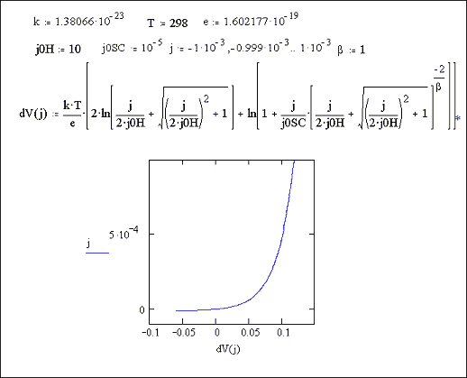
Figure 7.5 – Equation 7.16
plotted for the current density range –1 ´ 10-3 A cm-2
to 1 ´ 10-3 A cm-2
Case where |j0H| >> |j|
7.3.1.2 The case where |j| >>
|j0H|
For the case where |j|
>> |j0H|,
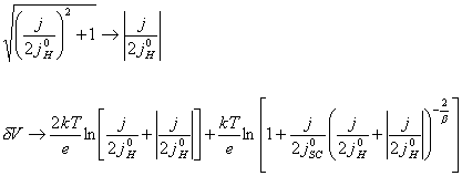
(equation
7.18)
For positive j:
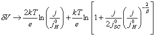 (equation
7.19)
(equation
7.19)
For negative j:
![]() (equation
7.20)
(equation
7.20)
Therefore, at negative
potentials, the current density is independent of the applied potential.
Figures 7.6 and 7.7 show a Mathcad plots of equation 7.16 for the case where |j0H| << |j|. Figure 7.6 shows the case for b = 1. Figure 7.7 shows the case for b = 1000.
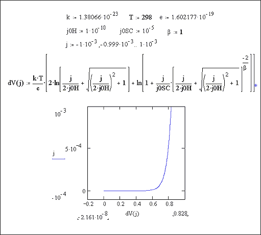
Figure 7.6– Equation 7.16 plotted for the current range -1 ´ 10-3 A cm-2 to 1 ´ 10-3 A cm-2 Case where |j0H| << |j|, b = 1
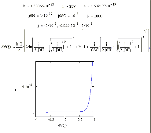
Figure 7.7– Equation 7.16
plotted for the current range -1 ´ 10-3 A cm-2 to 1 ´ 10-3 A cm-2 Case where
|j0H| << |j|, b = 1000
7.3.1.3 The case where |j0SC| >> |j| and j »
j0H
For the case where |j0SC| >>
|j|
and j » j0H,
equation 7.16 simplifies to equation 7.21.
 (equation
7.21)
(equation
7.21)
Figure 7.8 shows a Mathcad plot of equation 7.16 for the case where |j0SC| >> |j|. The behaviour is independent of b and is classic metal behaviour.
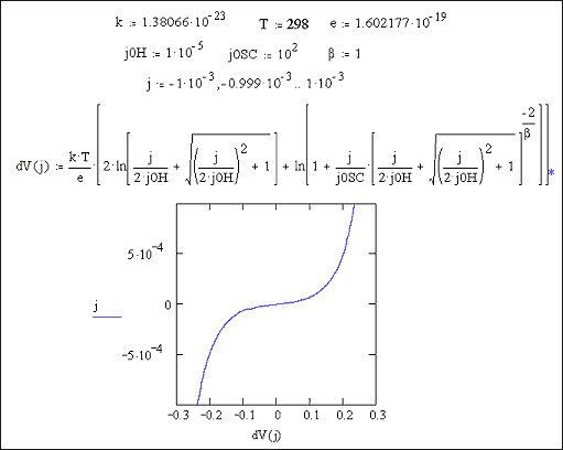
Figure 7.8– Equation 7.16 plotted for the current range -1 ´ 10-3 A cm-2 to 1 ´ 10-3 A cm-2 Case where |j0SC| >> |j|
7.3.2 The current density - applied potential
relationship at intermediate values
At high doping levels, j0SC will be high.
Metal behaviour will therefore be observed.
Reducing the doping level,
implies that j0SC
will become more significant and semiconductor behaviour would be expected.
Figures 7.9 and 7.10 show Mathcad plots of equation 7.16 over current density ranges of -1 ´ 10-4 A cm-2 to 1 ´ 10-4 A cm-2 and –1 ´ 10-3 A cm-2 to 1 ´ 10‑3 A cm-2 respectively. For both plots values of j0H = 1 ´ 10-5 A cm-2 and j0SC = 1 ´ 10-1 A cm-2 were used.
Figures 7.11 and 7.12 show Mathcad plots of equation 7.16 with various different values for the constants j0H, j0SC and b.
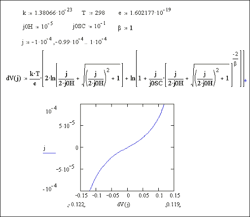
Figure 7.9 – Equation 7.16
plotted for the current range -1 ´ 10-4 to 1 ´ 10-4 A Number of surface states =
1013, Helmholtz capacitance
= 1 mF
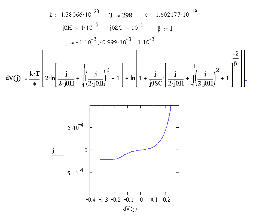
Figure 7.10 – Equation 7.16
plotted for the current range -1 ´ 10-3 to 1 ´ 10-3 A Number of surface states =
1013, Helmholtz capacitance
= 1 mF
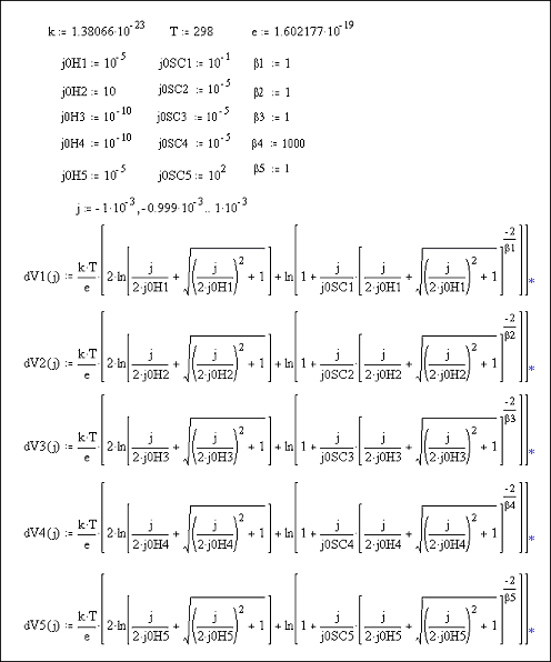
Equations and constants used
to plot Figures 7.11 and 7.12
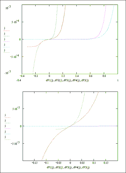
Figures 7.11 & 7.12 – Mathcad plots of equation 7.16.
7.4 AC Impedance and the Surface State Model
The surface state model can
be extended to consider small amplitude modulations (symbolised by overtilde embellishments):
![]() (equation
7.22)
(equation
7.22)
Applying Kirchhoff’s law:
![]() (equation
7.23)
(equation
7.23)
![]() (equation
7.24)
(equation
7.24)
The general equation for the
current density across Helmholtz current, jH,
is:
(see § 4.4.4, equation 4.8)
![]() (equation
7.25)
(equation
7.25)
Applying a small modulation
gives:
![]() (equation
7.26)
(equation
7.26)
Simplifying using the
following identities:
![]() , exp(x) ≈ 1 + x and cosh2 x = sinh2 (x +
1)
, exp(x) ≈ 1 + x and cosh2 x = sinh2 (x +
1)
gives ![]() (equation
7.27)
(equation
7.27)
For a steady DC current, j = jH
![]() (equation 7.28)
(equation 7.28)
A general equation for the current density across the space charge layer can be
derived from equations 4.18 and 7.9.
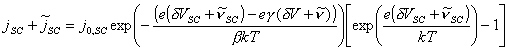
(equation
7.29)
Expanding for small
perturbations:
exp(x) ≈ 1 + x, exp(y) ≈ 1 + y xy → 0
![]()
(equation
7.30)
For a steady DC current, j = jSC
![]()
(equation
7.31)
![]() (equation
7.32)
(equation
7.32)
where ![]() and
and 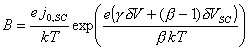
(equations
7.33 and 7.34)
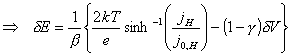
For a particular potential, j, b, j0,H and dVSC are all constant.
dV, dVSC and j can be determined from steady-state experiments.
Equations 7.22 and 7.32 can
be combined in order to lead to an expression which eliminates ![]() and
and ![]() .
.
Equation 7.22: ![]()
![]() where
where ![]()
(equations
7.35 & 3.36)
![]() (equation
7.37)
(equation
7.37)
![]() (equation
7.38)
(equation
7.38)
Substituting equation 7.38
into equation 7.22 gives:
![]() (equation
7.39)
(equation
7.39)
Substituting equation 7.37
into equation 3.65 gives:
![]() (equation
7.40)
(equation
7.40)
![]() (equation
7.41)
(equation
7.41)
Substituting equation 7.22
into equation 7.39 gives:
![]()
(equation
7.42)
![]()
(equation
7.43)
Substitute for ![]() ((equation 7.41) in the equation 7.43:
((equation 7.41) in the equation 7.43:
(equation
7.44)
![]() (equation 7.45)
(equation 7.45)
Which leads to an expression
for the impedance:
![]() (equation
7.46)
(equation
7.46)
![]() (equation 7.47)
(equation 7.47)
In Summary:
![]() (equation 7.47)
(equation 7.47)
where
![]() (equation
7.33)
(equation
7.33)
 (equation 7.34)
![]() (equation
7.36)
(equation
7.36)
![]() (equation
7.3)
(equation
7.3)
![]() (equation
7.7)
(equation
7.7)
If ![]() then g will tend to unity (γ → 1).
then g will tend to unity (γ → 1).
Considering the case where j = 0, the expression in equation 7.47 simplifies to:
![]() (equation 7.48)
(equation 7.48)
![]() (equation 7.49)
(equation 7.49)
This expression for Z forms
two semicircles when plotted in the complex plane. The first semicircle has a
radius of 1/B with a maximum, wmax, of B/CSC. The
second semicircle has a radius of 1/D
and a maximum, wmax,
of D/CH.
When not at open circuit
potential, the behaviour is slightly more complicated and it is necessary to
find values of j, dV and dVSC from DC experiments.
In Summary:
![]() (equation 7.49)
(equation 7.49)
where
 (equation 7.34)
![]() (equation
7.50)
(equation
7.50)
![]() (equation
7.51)
(equation
7.51)
Figure 7.13 shows a current
density – potential plot for a given set of parameters. That the curve passes through the origin and
the currents are significant for both small positive potentials and small
negative potentials. This would correspond to a system where the current
density was transport controlled and reversible cyclic voltammetry would be
observed.
Figure 7.14 shows an
impedance calculation at open circuit. Two semicircles can be seen. Figure 7.15 shows various impedance curves
taken for various j, dV values taken from the plot
in figure 7.13.
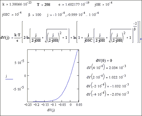
Figure 7.13 – current density / potential plot
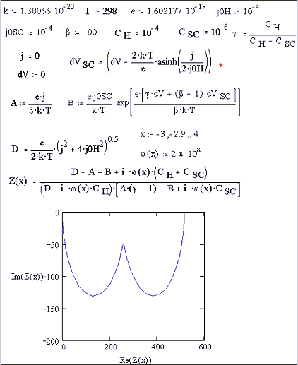
Figure 7.14 – impedance plot for open circuit conditions
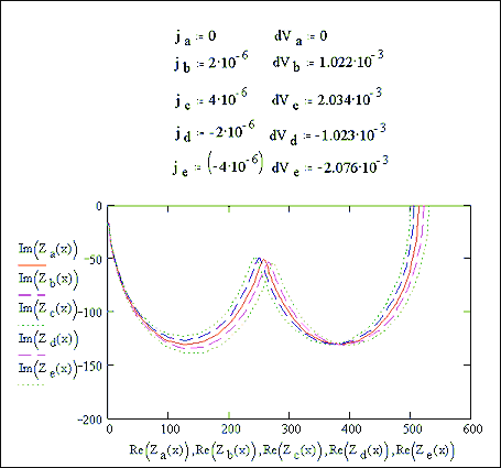
Figure 7.15 – impedance plots at various potentials
7.5 Interpreting the
Semiconductor Behaviour of Low Doped Diamond
The chapter 6 showed that
low doped diamond films, with boron concentrations of the order of 1019
cm-3, exhibited semiconductor behaviour.
For oxygen terminated
diamond films, cyclic voltammograms of well known redox couples were
irreversible with no defined reduction peaks. The diamond electrode acts as a p‑type
semiconductor. At negative applied potentials, the p‑type semiconductor
is reversed biased and the current density will be limited.
For hydrogen terminated
diamond films, the valence band is at a higher energy. The valence band minimum
at the surface is higher than the Fermi level (see figure 7.1). Accumulation of holes at the surface may
occur and so both anodic and cathodic reactions are possible.
7.6 Summary
The standard theories for
metal or semiconductor electrochemistry, as outlined in chapter 4, are not
sufficient to provide a model for the electrochemistry of boron doped polycrystalline
diamond films.
The mechanism of charge
transfer must be considered. The presence of surface states explains the
difference in behaviour between hydrogen and oxygen terminated diamond films.
A relationship between the
current density and applied potential has been derived. This agrees with the
experimental results, which show that metallic behaviour predominates in highly
doped diamond samples, while semiconductor behaviour is seen in low doped
samples.
The surface state model was
applied to the AC impedance studies and an expression was obtained that
predicts the two time constants that have been seen in the experimental
results.