Chapter 2 - Analytical Techniques
2.1
Introduction
Material characterisation in CVD diamond has been vital in sustaining progress in its development, especially so in recent years. Nowadays, there is easy access to highly efficient, fast and extremely sensitive analytical tools to distinguish diamond from any other forms of non-diamond carbon Such tools include X-ray photoelectron spectroscopy (XPS), X-ray diffraction, low energy electron diffraction (LEED), electron energy loss spectroscopy (EELS), secondary ion mass spectrometry (SIMS), and transmission electron microscopy (TEM) - by far the most powerful technique in establishing the detailed microstructure of a CVD diamond film (Details of how each of these techniques operate can be found in ‘Physical Methods for Materials Characterisation’, by P.E.J. Flewitt and R.K. Wild, B. Cantor ed., IOP Publishing Ltd. 1994, and references therein). Secondary ion mass spectrometry (SIMS) cannot distinguish between the different forms of carbon, but as a means to obtain a spatial distribution of different elements that may be present within a few atomic layers of a surface. This is particularly beneficial when explore the interfacial layer between the CVD diamond film and the non-diamond substrates. The three characterisation methods mainly used in the present work are discussed, namely
n Scanning Electron
Microscopy (SEM),
n Laser Raman
Spectroscopy (LRS), and
n Auger Electron
Spectroscopy (AES).
2.2 Scanning
Electron Microscopy (SEM)
The scanning electron microscope is a powerful tool for the examination of bulk specimens. Electrons are generated by thermionic emission from a tungsten filament heated to temperatures approaching 3000°C. These are then focused onto the sample surface. A detector then collects secondary electrons emitted from the surface of the specimen. An image is then formed on a cathode-ray tube (CRT) display.
Inspection of the
SEM micrographs can provide valuable information on the topology of the diamond
films:
n Top View - the
average grain size as well as the surface morphology of the deposited films,
n Cross-sectional
View - the film thickness and roughness.
However, such images, in themselves,
do not prove whether the films are diamond.
2.3 Laser
Raman Spectroscopy (LRS)
Laser Raman spectroscopy is the most widely used
technique to identify the characteristic energies of the chemical bonds or to
distinguish between different phases within the same material. For this reason it is a decisive tool for
establishing that the film is indeed diamond and for providing some measure of
the film quality. The Raman effect is
an interaction between monochromatic light, such as from a laser source, and
the chemical bonds within a specimen which produces a result that is similar to
infra-red absorption. When the laser
strikes the specimen, a small number of photons may excite molecular vibrations
in the specimen. Consequently, these
photons will be scattered with a slightly lower energy. Lasers of different excitation wavelengths
were used in the present work (632.8 nm - (red)
He/Ne laser; 514.5 nm - (green) Ar+
laser, and 325 nm - (ultra-violet) He/Cd
laser).
The Raman
spectrum of natural diamond shows a sharp, single peak centred at an wavenumber
of ~ 1332cm-1 (Figure 2.1).
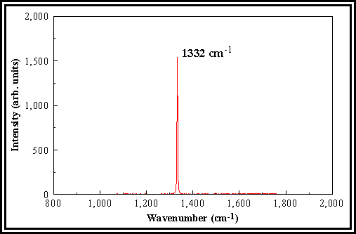
Figure 2.1. Laser Raman spectrum of natural diamond
showing the characteristic sharp peak at 1332 cm-1.
This
feature also dominates the Raman spectra of high quality, polycrystalline
diamond film grown by CVD methods (See Appendix III in Section 7.6,
Chapter 7, for examples). However,
additional peaks may be observed in the spectra which are characteristic of
non-diamond contamination, depending on deposition conditions (such as films
grown using high methane concentrations in the gas phase). The Raman spectrum of graphite shows a broad
feature centred around 1580 cm-1. When characterising CVD ‘diamond’ films, the observation of any
broad resonance at this higher wavenumber is generally taken to indicate the
presence of graphite-like non-diamond phases containing sp2-bonded carbon atoms.
The
full width half maximum (FWHM) of the 1332 cm-1 Raman line is
another measure of film quality; good quality CVD diamond films normally
produces peaks with a FWHM of 4-10 cm-1, whilst linewidths in the
region of 2-2.5 cm-1 are characteristic of natural
diamond. CVD diamond can only produce
linewidths close to those of natural diamond if the films are non-continuous,
giving rise to separate diamond crystals.
2.4 Auger
Electron Spectroscopy (AES)
Auger
Electron Spectroscopy or AES is a useful technique for the compositional
analysis of surfaces. Like secondary
electrons, Auger electrons are emitted when an electron beam bombards a sample. However, the emission process is different,
as is illustrated in Figure 2.2. An
incoming electron can ionise an atom in the material, and leave a ‘hole’
(Figure 2.2 (a) ). If this electron is
from an inner shell of the atom, internal rearrangement of electrons may take
place, resulting in an electron in an outer shell falling into the hole (Figure
2.2 (b) ). The energy emitted by this
process may either be released as an X-ray, or used to eject another less
tightly bound electron (Figure 2.2 (c) ).
The latter process is known as Auger emission, and the electron known as
the Auger electron. The energy of the
Auger electron is characteristic of the material. As Auger electrons have low kinetic energy, only those within
5 nm of the surface can contribute to observable emission. Thus the Auger process is useful in
providing surface chemical information.
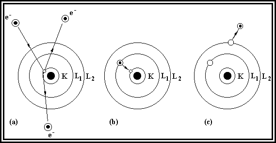
Figure 2.2. The Auger process.