Appendix B - Bias Enhanced Nucleation
“aut amat aut odit mulier, nihil est tertium”
Syrus
B.1 Introduction
The technique of bias-enhanced nucleation (BEN), was briefly introduced in Section 1.7. Some limited work was performed in this area, as an aside to the main work in this thesis, during times when experimental problems hindered us performing molecular beam mass spectrometry (MBMS) experiments. The BEN technique, pioneered by the team of Yugo et al in 1990 [[1]], is conceptually straightforward - an electrical bias is applied to an otherwise untreated electrically conducting substrate, under similar conditions to CVD diamond growth, for a short period (a few minutes to several hours) prior to actual deposition. This treatment was found to produce a vast increase in nucleation density (number of diamond crystallites formed per unit area) from 103-105 cm-2 (pristine Si) [[2],[3]] to >1010 cm-2 [3,[4]] (BEN). Typically, for comparison, manual abrasion can achieve a nucleation density ~107 cm-2 [4]. The bias applied to the substrate is usually negative d.c. of ~200 V magnitude, with respect to an anode (which in many cases is the grounded CVD chamber walls). The advantage of the process is that it allows the user to nucleate diamond without the need to mechanically damage the substrate, as is the case for manual abrasion, for example. This ability is important if CVD diamond is to find use in microelectronic devices, or many optical applications.
Early researchers in this field noted that the process had the drawback of poor reproducibility [[5]], and high nucleation densities would only occur over small areas of the substrate surface [[6]]. Also, the precise conditions needed for successful BEN appeared to depend critically on the reactor layout (electrode configuration, chamber dimensions) and CVD parameters used, implying the need for extensive characterisation of a given type of reactor to reach optimal BEN conditions.
B.2 Experimental Details
In order to set up the BEN system, it was decided that the most convenient electrode configuration was to negatively bias the substrate holder casing (the holder was designed with an extra vacuum feedthrough for such a purpose), relative to the CVD chamber walls (which are always earthed for safety). A schematic diagram of the BEN system is shown in Fig. B.1.
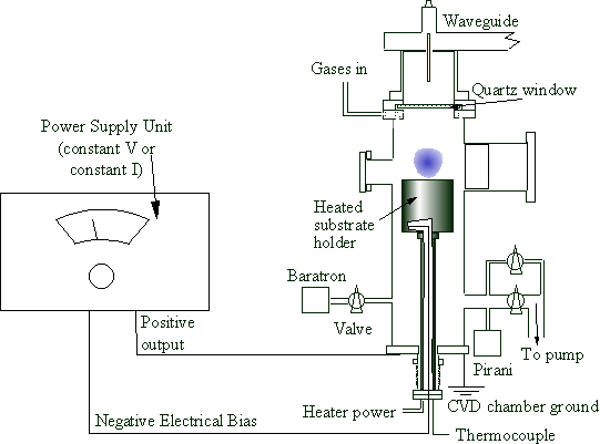
Figure B.1 Schematic diagram showing the MWCVD reactor adapted for BEN.
BEN is generally carried out under similar conditions to diamond CVD, but prior to the deposition. Typically, an enriched carbon feed is used, often ~2-5% CH4/H2 [3,4, 6,[7]], but sometimes as high as 15% [[8],[9]]. Other studies found it beneficial to instead use a pre-bias carburisation step, where a short period (~1 hour) of CVD diamond growth was carried out on the otherwise untreated wafer under comparatively CH4 rich conditions (2-5%), before application of the bias voltage [[10],[11]]. During BEN, other CVD parameters (reactor pressure, microwave power etc.) are generally set at the same values to be used for the diamond growth step. For all the BEN studies in this appendix, 2% CH4/H2 was used, and 1000 W microwave power, 20 Torr pressure, and 700°C substrate temperature (as read by the thermocouple in the substrate holder). Growth was carried out under identical conditions to BEN, except the CH4 mole fraction was lowered to 1%.
Two different power supply units (PSU’s) were used for the electrical bias. These were an Airco Temescal CL-2A 0-2 kW constant current glow discharge power supply, and a Brandenburg Series 4000 constant voltage power supply. Initially we used the Brandenburg constant voltage unit, as this was the type of PSU (constant voltage) used most prevalently in the literature.
B.3 The Effect of the BEN process
High resolution electron microscopy and atomic force microscopy studies of Si wafers which have undergone carburisation and/or BEN steps show the development of an interfacial SiC layer, the surface texture of which retains some registry with the crystallographic orientation of the Si lattice underneath [[12],[13]] (see Fig. B.2). It is believed that as this layer thickens, its surface becomes carbon rich, forming amorphous carbon islands, and subsequently local areas of sp3-bonding which grow to form diamond nuclei of nanometre dimensions.
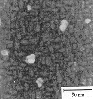
Figure B.2 High resolution SEM image of Si wafer which has undergone a typical BEN treatment, taken from ref. [12], showing the textured interfacial layer, with small nucleated diamond crystals.
The diamond crystallites nucleated during BEN are sometimes oriented with the texture of the SiC layer, and hence the Si wafer underneath [10,11,[14]]. This causes diamond crystals formed during BEN to align with the crystallographic planes of the Si substrate, allowing growth of ‘oriented’ diamond particles and films. Oriented, polycrystalline, diamond films have one particular crystal facet parallel to the substrate surface, and hence can be made very smooth. This would be beneficial for many applications of CVD diamond technology as it allows growth of smooth diamond surfaces (optics applications), or heteroepitaxial single crystal growth (microelectronics applications). Smooth CVD diamond surfaces do not require much finishing, such as the lapping and polishing which is required for randomly oriented CVD diamond.
B.4 Effect of Bias Voltage
When the bias voltage is applied to the substrate holder casing, the plasma ball moves slightly closer to the substrate, and an additional, flat, pancake-shaped plasma (~1 mm thick) often appears ~1 mm above the substrate surface. The ‘pancake’ was brighter, and larger in extent when using negative bias voltages, than when using positive voltages, where the pancake was smaller, fainter, or even non-existent. The pancake plasma increased in brightness as the magnitude of the voltage was increased. Some authors have noted that the pancake plasma moves across the substrate, and that the visible edge of the pancake roughly correlates with the extent of high nucleation densities [[15]].
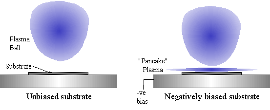
Figure B.3 Effect of electrical bias on plasma appearance.
The Brandenburg PSU was used to carry out BEN, and the effect of bias voltage examined in the range +165 V to -320 V (the maximum voltage magnitudes the PSU could provide whilst maintaining a stable plasma). In order to determine the nucleation density, it is usual to carry out the BEN process, followed by a short period (typically ~0.5-3 hours) of CVD diamond film growth (under identical conditions to BEN, except 1% CH4 and, of course, no bias!). This allows all nucleated diamond crystals formed during BEN (~ nm scale) to grow to a size where they are easily identifiable in typical scanning electron microscopes (>100 nm). The number of diamond crystallites visible on the SEM image is counted up, and divided by the area (deduced from the SEM image scale bar) to give the nucleation density. The results of this study are shown in Fig. B.4. Also included are the results of Kulisch et al [6], and McGinnis et al [3] who performed a similar studies and found that the nucleation density achievable increases dramatically as a function of bias voltage, V.
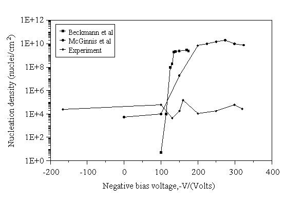
Figure B.4 Effect of bias voltage on the nucleation density of diamond crystals on mirror-polished Si wafer substrates. The results of Kulisch et al [6], and McGinnis et al [3], are also shown for comparison.
The present results do not show the nucleation enhancement seen by other authors as the bias voltage is increased. A possible explanation for this can be seen by considering these findings in the light of further results from the paper of Kulisch et al [6], where the bias circuit current-voltage (I-V) characteristic was investigated. Three behavioural regimes were identified, and are shown in Fig. B.5, along with the I-V characteristic measured in the present work. Under conditions of zero bias, ions in the plasma have thermal energies (as they are too massive to respond to the time dependent electric component of the microwave field, and hence only exchange energy during collisions with other molecules). The effect of the electrical bias is to accelerate positive ions in the plasma toward the substrate. In region I, the current of positive ions to the substrate is mobility limited. That is, the energy gained from bias voltage acceleration is not large enough to accelerate all (positive) ions to the substrate surface, as the ions lose energy, and indeed may be destroyed, by collisions during transit from the bulk plasma to the substrate. In region II, the larger bias voltage means that all ions have enough energy to make the transit from plasma to substrate, thus current saturation behaviour is observed. In region III, ions gain significant energy from the accelerating bias voltage and may cause additional ionisation through energetic collisions on their way to the substrate, increasing the ion flux (i.e. current) arriving at the substrate surface. Kulisch et al noted that it is best to carry out BEN in region III, as this is where the increase of nucleation density is seen to occur [6] (see Fig. B.4).
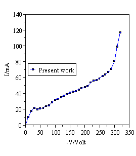

Figure B.5 Current-voltage characteristic of bias circuit. The results of Kulisch et al [6] are shown for comparison. Regions I-III are explained in the text.
The present current-voltage relationship shows that even at the most negative bias voltage it was possible to attain, region III was still not reached, explaining the comparatively low nucleation densities observed. Further, this suggests that to achieve enhanced nucleation, it would be better to use a more negative voltage than -320 V. If the bias was made more negative than 320 V, the plasma started to flicker and become unstable. It was therefore decided to attempt BEN using the constant current Airco glow discharge PSU (Section B.5).
Furthermore, we did not observe the current-time (I-t) characteristic seen by Kulisch et al [6]. This is shown in Fig. B.6, along with the experimentally observed result. Kulisch et al were able to interpret their I-t relation in terms of how the chemical composition of the growth surface was changing during the bias process. They attributed rises in the bias current to SiC deposition, and later to hydrocarbon deposition as amorphous carbon (a-C), and to the formation of diamond ‘nuclei’.

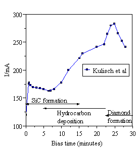
Figure B.6 Typical current-time characteristic measured for the bias circuit. The results of Kulisch et al (right, adapted from [6]), and their interpretation of the observed current changes which they observed is also given.
These evolutionary stages had been seen by other authors [15,[16]], but the magnitude of the current rises differed considerably. Enhanced currents have been observed from diamond coated substrates [6], and it is believed that secondary electron emission from diamond surfaces in the vicinity of the substrate causes this effect. Schreck et al found the bias current to rise by a factor of 10 during BEN on formation of diamond nuclei [16], whilst Kulisch et al [6] recorded a 60-70% increase, and Stöckel et al observed only a modest 20% increase [15]. These discrepancies were explained by considering the geometry of the plasma-substrate interface, and the effect substrate size and proximity to the plasma had on the ion current arriving at the substrate. Schreck et al used a 30 mm diameter substrate raised 2-4 mm into the plasma bulk, whilst Kulisch et al used a three inch diameter substrate several millimetres below the visible edge of the plasma. Stöckel et al located their 10 mm2 substrate on a much larger diamond coated substrate holder, again several millimetres below the visible edge of the plasma. Therefore the current arriving at the substrate would be expected to be higher for the experiment of Schreck et al, as it is a comparatively large substrate in contact with the plasma. The experimental arrangement of Stöckel et al was most akin to that employed in the present work, thus it would be expected that any current rise observed with the present BEN system would only be very small. No such increases in bias current were observed in the present study - this complements the fact that no nucleation enhancement was found. Even raising the substrate into the plasma bulk using a ~3 mm thick Mo plate did not noticeably change the observed nucleation density. Moreover, Raman spectra of the Si wafers which had been subjected to the BEN process do not show any features which may be attributable to carbon - only the first order Si Raman peak at 520.1 cm-1, and the second order Si feature are visible. Isolated CVD diamond crystals were formed, but no more than would be expected on virgin Si.
Figure B.7 Raman spectra of a) Si wafer surface after XXX minutes BEN at XXX V. b) Isolated diamond crystal formed during the same deposition.
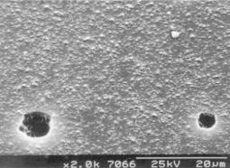
It is also worth examining the Si surface morphology as a function of bias voltage. As the magnitude of the negative d.c. bias was increased, the Si wafer began to show comparatively large (~10mm) etch pits, and roughening on a micron scale (Figs. B.X-B.X). This was most likely due to the effect of positive ion bombardment from the plasma.
a) b)
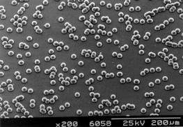
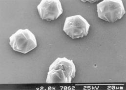
Figure B.Xa & b: SEM image of diamond crystallites formed by BEN. Conditions: 220 min bias at -160 V followed by 3.0 h CVD diamond growth (Sample B4).
a) b)
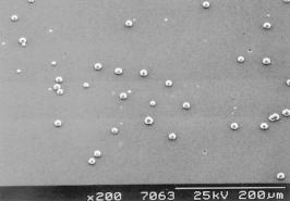
Figure B.X SEM image of diamond crystallites formed by BEN. Conditions: 20 min bias at +165 V followed by 180 min CVD diamond growth (B9).
a) b)
Figure B.X Effect of prolonged, high voltage biasing. SEM image of diamond crystallites formed by BEN. Conditions: 258 min bias at -250 V followed by 105 min CVD diamond growth (B12).
Ion bombardment of the substrate is not a significant problem in unbiased microwave plasma systems as ions have a thermal energy distribution. When a negative bias has been applied to the substrate, positive ions gain more energy from the applied d.c. potential drop, and are accelerated toward the substrate, arriving with greater than thermal energy. This results in the observed etching effects. Ion energy distributions have been measured using a retarding field probe by Robertson et al [8], and are found to peak at 50 eV at -200 V bias, increasing to 120 eV at -290 V. This ‘hyperthermal’ ion bombardment is believed to cause ‘subplantation’ of ions into the top few atomic layers of the SiC interface [[17]], being energetically sufficient to keep the deposit amorphous.
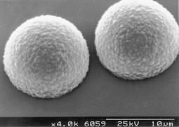
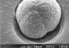
The diamond crystallites formed during BEN are roughly spherical with visible faceting. These crystallites can reach 20 mm in size after ~3 hours growth (Fig. B.X), which is greatly in excess of the diameter predicted from the diamond film linear growth rate (~0.3 mm h-1´3 h = ~1 mm) which would be observed for normal CVD growth under the same conditions These crystallites have been shown to be diamond by Raman spectroscopy (Fig. B.X). It was not possible to determine from the present data whether this increased growth rate was due to the electrical bias, or whether isolated crystals grew quicker than CVD diamond films. Schreck et al [[18]] have shown that a -200 V electrical bias maintained throughout normal CVD diamond growth increases the obtainable growth rate by a factor of four over that obtained in the absence of electrical bias, so their results lend support to an enhanced growth rate during biasing.
Figure B.X Raman spectrum of a typical diamond crystallite nucleated by BEN. 633 nm laser excitation. Bias conditions: 1000 W, 20 Torr, 700°C substrate temperature, 2% CH4/H2. Growth conditions: 1000 W, 20 Torr, 700°C substrate temperature, 1% CH4/H2.
B.5 Effect of Bias Current
BEN was also attempted using the Airco PSU. As this supplied a constant current, the bias voltage was monitored as a function of time for various bias currents. Only a few BEN runs were attempted using this PSU. Typical bias voltage-time (V-t) characteristics obtained are shown in Fig. B.X.

Figure B.X Typical voltage-time characteristics obtained when using a constant current PSU for the electrical bias.
Using this arrangement, we did not always see a wide ‘pancake’ plasma, rather the second discharge appeared to be concentrated at a corner of the substrate, and would slowly move to cover it over the course of several hours. This is the type of behaviour which other authors have ascribed to diamond nucleation during BEN. When such samples were subjected to a CVD diamond growth step it was found that a continuous film of ~5 mm2 could be grown in the region directly under the pancake plasma. SEM images of such deposits are shown in Fig. B.X.
It is clear that the constant current power supply was more successful at allowing the nucleation of diamond than the constant voltage supply, although there is no apparent reason why this should be so.
B.6 Conclusions
As this was purely an aside to the main work in this thesis, a comprehensive study and optimisation of the BEN process was not possible. The effect of bias voltage and current were examined, but successful growth of diamond films with high (~1010 cm-2) nucleation density were not achieved. This was believed to be due to the non-optimal parameters employed for other variables (bias time, CH4 mole fraction in feed, pressure). In order to get the process to work on the present system, a large scale study would be necessary to optimise all the relevant variables (this is the approach that all other BEN research groups have had to take to get their individual BEN systems to work in different reactor geometries). It would also be necessary to ensure good electrical contact between the wafer and substrate holder, which was hindered by the CVD diamond coating on the latter. It may also be beneficial to carry out the bias at lower pressures (~15 Torr) as this has been shown to result in larger bias currents [[19]].
Partial success was found when using the constant current PSU, in that a continuous coating was observed over a small area (~5 mm2). Raman spectroscopy, however showed this to be graphitic in nature (?).
B.7 References