“How profound that mystery of the Invisible is! We cannot fathom it with our miserable senses, with our eyes which are unable to perceive what is either too small or too great, too near to us, or too far from us”.
Guy de Maupassant, ‘The Horla’ (1887).
2.1 Introduction
This chapter contains descriptions of the main techniques used to characterise the diamond films grown in this work. Laser Raman spectroscopy, and scanning electron microscopy were the two main techniques used for diamond film characterisation. Secondary ion mass spectrometry is also mentioned briefly, as some measurements were taken from our films using this technique by Dr Rego of Manchester Metropolitan University.
2.2 Laser
Raman Spectroscopy (LRS)
Raman spectroscopy is a useful technique for the identification of a wide range of substances - solids, liquids, and gases. It is a straightforward, non-destructive technique requiring no sample preparation. Raman spectroscopy involves illuminating a sample with monochromatic light and using a spectrometer to examine light scattered by the sample.
At the molecular level photons can interact with matter by absorption or scattering processes. Scattering may occur either elastically, or inelastically. The elastic process is termed Rayleigh scattering, whilst the inelastic process is termed Raman scattering. The electric field component of the scattering photon perturbs the electron cloud of the molecule and may be regarded as exciting the system to a ‘virtual’ state. Raman scattering occurs when the system exchanges energy with the photon, and the system subsequently decays to vibrational energy levels above or below that of the initial state. The frequency shift corresponding to the energy difference between the incident and scattered photon is termed the Raman shift. Depending on whether the system has lost or gained vibrational energy, the Raman shift occurs either as an up- or down-shift of the scattered photon frequency relative to that of the incident photon. The down-shifted and up-shifted components are called respectively the Stokes and anti-Stokes lines. A plot of detected number of photons versus Raman shift from the incident laser energy gives a Raman spectrum. Different materials have different vibrational modes, and therefore characteristic Raman spectra. This makes Raman spectroscopy a useful technique for material identification. There is one important distinction to make between the Raman spectra of gases and liquids, and those taken from solids - in particular, crystals. For gases and liquids it is meaningful to speak of the vibrational energy levels of the individual molecules which make up the material. Crystals do not behave as if composed of molecules with specific vibrational energy levels, instead the crystal lattice undergoes vibration. These macroscopic vibrational modes are called phonons.
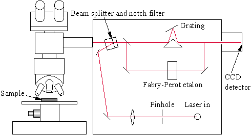
Figure 2.1 Schematic diagram of a Raman spectrometer.
In modern Raman spectrometers (Fig. 2.1), lasers are used as a photon source due to their highly monochromatic nature, and high beam fluxes. This is necessary as the Raman effect is weak, typically the Stokes lines are ~105 times weaker than the Rayleigh scattered component. In the visible spectral range, Raman spectrometers use notch filters to cut out the signal from a very narrow range centred on the frequency corresponding to the laser radiation. Most Raman spectrometers for material characterisation use a microscope to focus the laser beam to a small spot (<1-100mm diameter). Light from the sample passes back through the microscope optics into the spectrometer. Raman shifted radiation is detected with a charge-coupled device (CCD) detector, and a computer is used for data acquisition and curve fitting. These factors have helped Raman spectroscopy to become a very sensitive and accurate technique.
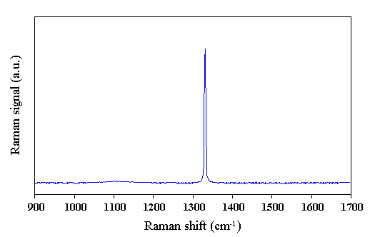
Figure 2.2 Raman spectrum of natural diamond (type IIa), showing the main Raman active mode at ~1332 cm-1 (Taken using 514.5 nm laser excitation wavelength). The Raman signal intensity is in arbitrary units (a.u.).
Natural diamond exhibits one main Raman active vibration which manifests itself as a sharp first order peak in the Raman spectrum at ~1332 cm-1 in natural diamond and a weak second order feature at ~2750 cm-1 [[1]]. A Raman spectrum taken from a natural diamond sample, showing the first order peak, is presented in Fig. 2.2. The first order peak is well fitted with a Lorentzian line shape, the full-width at half the peak height (FWHM), is typically £2 cm-1. In diamond films grown by CVD, carbon is also incorporated into the film in non-diamond forms. These non-diamond carbons may be graphitic [[2]-[4]] or amorphous carbon [3,4] regions in the film. The Raman spectrum of an infinite crystal of pure graphite (or a large single crystal sample, in practice) would show one sharp peak at 1580 cm-1 [3,[5]]. For small crystallite sizes, the selection rules concerning the Raman inactivity of certain phonons in infinite graphite crystals are relaxed as the crystal can no longer be regarded as infinite. The sharp graphite peak becomes a broad band (the G-band). and a ‘disordered’ (or D-band) peak appears in the spectrum at ~1350 cm-1 [5]. Amorphous carbon produces a broad asymmetric hump in the region 1000-1600 cm-1 [[6]]. Both graphite and amorphous carbon have Raman scattering efficiencies greater than that of diamond. This means that for identical numbers of sampled atoms in the three carbon forms - diamond, graphite, and amorphous carbon, the graphite and amorphous carbon samples would give a much larger Raman signal than the diamond sample. These scattering efficiency ratios, relative to diamond have been reported to be ~50 times for graphite [[7]], and ~233 times for amorphous carbon [[8]], both measured using 514.5 nm laser radiation. Diamond is highly transparent to visible laser radiation, whilst graphitic regions are not. The penetration thickness, or thickness through which the transmitted laser radiation may pass before its intensity reaches e-1 (~37%) of its incident value, is 50 nm for graphite using 488.0 nm laser radiation [5]. Hence Raman spectroscopy probes the bulk of transparent, good quality diamond. In poor quality samples, graphitic inclusions can ‘screen out’ the diamond signal from diamond regions deeper in the sample making the Raman spectrum indicate a worse quality film than is actually the case. A Raman spectrum typical of CVD diamond is shown in Fig. 2.3.
In addition, some features of the diamond Raman spectrum change their intensity and position as the laser excitation wavelength is varied [[9]-[14]]. Thus, the choice of laser wavelength used is important when obtaining Raman spectra. Diamond exhibits photoluminescence and this is also detected by the Raman spectrometer, with the Raman spectrum superimposed on it. It can be seen that the deconvolution and quantitative interpretation of CVD diamond Raman spectra is not a straightforward process.
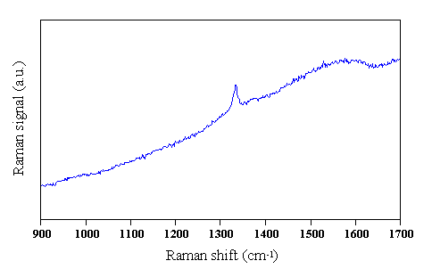
Fig. 2.3 Typical Raman spectrum obtained from a CVD diamond film, deposited using MWCVD from a 0.5% CH4/H2 gas mixture, 1000 W microwave power, 700°C substrate temperature for 6 hours. Raman spectrum taken using 514 nm laser excitation.
The features present in CVD diamond Raman spectra are used to give some feeling for the quality of the deposited film. A strong, narrow first order diamond peak, located at ~1332 cm-1, and a lack of features attributable to non-diamond carbons indicates that the film is of good quality. It is possible to curve fit the Raman spectra using computer packages, and by taking into account the scattering efficiencies for each peak to obtain a ratio for the volume of diamond to graphite in a sample. However, as mentioned in the previous paragraph, this is not a simple process, and generally not undertaken.
2.3 Scanning
Electron Microscopy (SEM)
Electron microscopies form the most widely used surface characterisation methods. A detailed explanation of the technique of SEM can be found in [[15]]. SEM, as it’s name suggests, uses electrons instead of light to image a sample. The electrons are generated by thermionic emission from a metal filament, and accelerated to ~25 keV. A system of electrical and magnetic field ‘optics’ is used to focus the beam to a spot ~10 nm in diameter on the sample surface. A schematic of a typical scanning electron microscope is shown in Fig. 2.4.
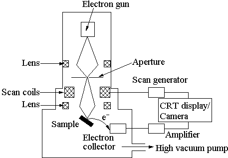
Figure 2.4 Schematic diagram of a Scanning Electron Microscope.
The sample surface must be electrically conducting, otherwise the electron beam would charge up the surface. As diamond is an insulating material, the sample is given a thin (~10 nm) Au coating by glow discharge sputtering before SEM examination. SEM must be carried out under a high vacuum (10-6 Torr or better). The electron beam is scanned, or ‘rastered’ across the sample via magnetic scan coils. The current of electrons reflected from the surface is collected, amplified, and plotted as a two-dimensional ‘micrograph’ image of the signal intensity. Features down to the spot size (~10 nm) may be resolved. As such, SEM can only give information on the appearance, or morphology, of the sample surface, and not definitive proof that the surface is (for example) diamond. By mounting the sample so it is viewed edge on its thickness can be measured. In the present work, this allows us to determine the growth rate of the diamond film, as we know the amount of time for which growth was carried out for.
2.4 Secondary
Ion Mass Spectrometry (SIMS)
This highly sensitive technique is used to analyse the chemical composition of materials, especially thin films. The technique is described fully in Chapter 7 of reference [15]; a brief explanation is given here. The sample under study is put under UHV and an ion gun used to bombard the sample surface with high energy ions of an element not present in the sample, usually an inert gas such as Ar+. These ions damage the sample surface by sputtering. A mass spectrometer is used to analyse the mass of species sputtered off the surface. This gives elemental composition information about species present in the sputtered region. Fig. 2.5 is a schematic of the ion bombardment process, and subsequent mass spectrometer detection of ionic species.
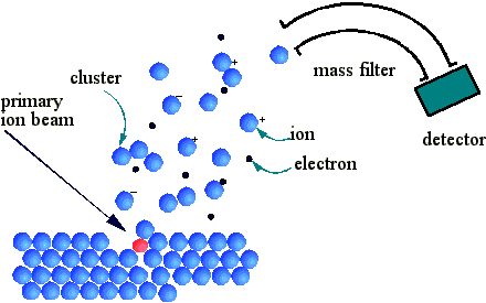
Figure 2.5 Schematic diagram showing the ion bombardment process and SIMS detection apparatus.
Since the sputtering process gradually removes material from the surface, SIMS can be used to provide a depth profile of relative species abundances. This technique is therefore useful for determining the presence of impurities, or dopant atoms in the diamond film bulk. Whilst not used routinely in the course of this thesis, SIMS data was obtained for samples grown with N2 added to a 1% CH4/H2 mixture. This was to measure the amount of nitrogen incorporated into the film bulk, and these results are given in Chapter 6.
2.5 References