
In the literature there is now a lot of evidence that the very low switch-on fields reported for the electron emission from diamond films appears to be due to geometric field enhancement. This is confirmed by the fact that boron-doped diamond tips have similar switch-on fields to nitrogen-doped films. Work presented by Mike Geis of MIT Lincoln Labs at the 1997 Diamond conference in Edinburgh showed that surface emission from the interface of the triple junction between metal, diamond and vacuum gave switch-on fields below 1V/µm, and so this offers potentially a new route to exploiting the electron emission properties of diamond.
The SCE mechanism is the one of interest here, since it offers a number of advantages over conventional field emission:
We are currently looking at two device structures to exploit SCE.
 We use p- or n-type nanogrit fabricated by crushing a diamond film previously grown by MWCVD. The diamond grit is then oxidised to remove any surface conducting graphite layer, then mixed into a slurry and deposited onto a Si substrate using an ink-jet printer. This allows structures with close to micron scale geometries to be realised. The surface is then rehydrogenated, and ohmic contacts are deposited. These devices give good switch-on thresholds (<10V/µm) with reproducible emission performance.
 This utilises p-type diamond on n+-silicon, and employs forward bias to switch on electron emission. We are currently testing the emission characteristics of such devices. By placing the current collecting anode either (a) above the diamond surface and (b) 100µm away from it (see diagram), we can measure current being emitted from the diamond surface itself or from the diamond-metal-vacuum interface.
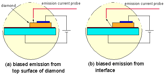 | Testing the emission properties of the heterojunctions from the diamond surface and the interface |
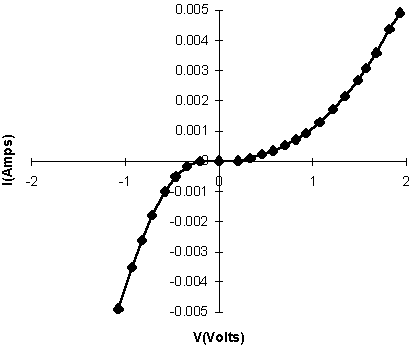 | Contact I-V plotted for the forward biased p-n junction |
We find that emission from the interface is better than that from the p-diamond surface, providing possible evidence of surface state emission. The I-V data fit a Riben-Feucht model for stepwise recombination and tunnelling across a junction via interface states. We observe that electron emission is initiated by a forward bias of around 1V. We hope to be able to extend these results to produce working SCE devices for use in displays in the near future.
For more information contact Dr Neil Fox Bristol Physics Dept or Professor Wang Wang, Bath Physics Dept.
 Back to Bristol University Diamond Group Home Page