Chapter 4
Electrochemical theory for diamond electrodes
4.1. Introduction
Diamond has been suggested
as a very attractive electrode material due to its remarkable properties
(outlined in chapter 1). The electrochemistry of diamond resembles that of a
metal. However diamond is a semiconductor. Standard theory cannot explain the
electrochemical behaviour of boron doped diamond.
After a basic review of
metal electrochemistry, a new theory to explain the electrochemical behaviour of
boron doped diamond is introduced that is based on surface state mediated electron transfer. The new theory is used
to predict the influence of changing doping density on the electrochemistry.
4.2. Metal Electrochemistry
Marcus-Gerischer theory1 as applied to basic electrochemistry at a metal
electrode2 is introduced in this section. The essential idea is
that the electron transfer occurs between occupied and unoccupied states that
are equal in energy 3.
The theory relates the
overpotential, h, to the total current
density, j, at the metal-solution
interface. This total current density is defined as the sum of the anodic
current density, ja, and
the cathodic density current, jc.
Cathodic current is considered negative by convention.
j = ja + jc [equation
4.1]
Anodic density current flows
when the oxidation process occurs at the electrode surface
R
→ O + e-
(e.g.
: Fe2+(aq)
→ Fe3+(aq) + e-)
Cathodic density current
flows when the reduction process occurs at the electrode surface
O + e-→ R
(e.g. : Fe3+(aq)
+ e- → Fe2+(aq))
To reduce difficulties in
the mathematical development the Frank-Condon approximation is applied to the
electron transfer process, i.e., the nuclei, being much heavier relative to
electrons, move slowly compared to electrons and can be considered as
stationary during the electron transfer process 4. The electrons are transferred to energy levels at or
near the Fermi level in the metal. In an electrochemical experiment a
modification in the applied potential results in charging of the metal, i.e., the metal surface potential is
modified. Therefore the Fermi level changes its position in the metal when the
applied potential is modified. However for a metal no modification occurs in
the occupation of the states about the Fermi level. Hence, current densities
are simply proportional to the overlap integral of the Fermi junction in the
metal and the density of the states function for the solution species:
ja µ (overlap of EF and ER)
jc µ - (overlap of EF
and EO)
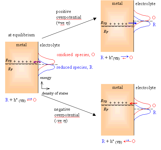
When the equilibrium
potential is reached, the overlap integrals are equal. Therefore the values for
ja and jc are equal in magnitude
with opposite sign. As a result the net current density is zero. (See figure
4.1, focus on the plot on the left side of the figure).
When the equilibrium is
perturbed and a positive overpotential (considering overportential as the
deviation of the potential from the equilibrium value 5) applied, the overlap integral for the reduced
electrochemical species is much bigger than for the oxidised species. An anodic
current flows and net oxidation occurs. (See figure 4.1, focus on the plot on
the upper right side of the figure).
When a negative overpotential
is applied the overlap integral for the oxidised electrochemical species is
much bigger that the same for the reduced species. The net current density is
negative. A cathodic current flows and reduction of the electrochemical species
occurs. (See figure 4.1, focus on the plot on the lower right side of the
figure).
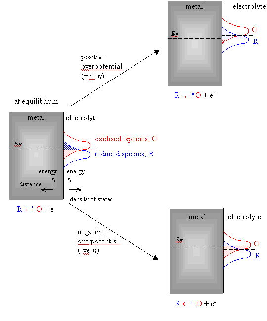
Figure
4.1. Schematic distribution functions on the rate of electron transfer for a
metal-solution interface.
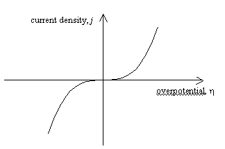
Figure 4.2 shows a sketch of
current density versus overpotential for electron transfer at a metal/ solution
interface. Current density and overpotential are related by the Butler-Volmer
equation.
![]() [equation
4.2]
[equation
4.2]
where j: current density R: gas constant
jo:
exchanged current density T: temperature
a: transfer coefficient h: overpotential
F:
Faraday constant
The plot shown in figure 4.2 assumes a = 0.5.
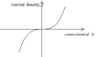
Figure
4.2. Current density – overpotential relationship for a=0.5
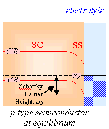
4.3. Ideal p-type Semiconductor Electrochemistry
In a p-type semiconductor
the majority change carriers are positive holes in the valence band.
Anodic reaction
R
+ h+(VB) → O
(e.g.: Fe2+(aq) + h+(VB)
→ Fe3+(aq))
Cathodic reaction
O → R + h+(VB)
(e.g.: Fe3+(aq) → Fe2+(aq)
+ h+(VB))
Unlike metals no states are
available at the Fermi level and charge transfer only occurs at the surface
energy of the valence band, EVB,S.
The anodic current that flows at the semiconductor electrode is dependent on the
surface concentration of majority change carriers and the overlap integral of EVB,S and ER:
ja µ (overlap of EVB,S
and ER) ´ ( [h+]surface ).
However, the cathodic
current is basically constant because the electron disposability remains
approximately constant.
jc µ -(overlap of EVB,S and EO).
When a positive
overpotential is applied (see figure 4.4., focus on the plot of the right upper
side on the figure), the thermodynamics indicates that the system is no longer
at equilibrium and oxidation will occur. However, to determine current
densities the rates of the reduction must be considered and not the
thermodynamics. If it is assumed that the overpotential is dropped across the
space charge layer, i.e. only band bending is modified and there is no change
in the overlap terms at the valence band edge. However, the concentration of
holes at the surface is increased.
Therefore
jc = jc,0 and ja > ja,0
where jc,0 is the
exchange cathodic density current and ja,0 is the exchange anodic
density current. The net positive current flux is positive. When a high
positive overpotential is applied the concentration of the holes at the surface
increases steeply (an exponential relationship between the surface
concentration and the overpotential applies) and ja >> ja,,0.
When a negative
overpotential is applied (see figure 4.4, focus on the plot on the right middle
side of the figure), the thermodynamics indicates that the system is no longer
at equilibrium and reduction will occur. Focusing on the current densities and
therefore on the rates of the reduction and oxidation process rather that the
thermodynamics, there is no change in the overlap terms at the valence band
edge but concentration of holes at the surface is decreased. Therefore
jc = jc,0 and ja < ja,0
that produces a net negative
current flux. When a high negative overpotential is applied the concentration
of the holes at the surface approaches zero and a limiting current density of jc,0 (a negative current) is
obtained.
When a very negative
overpotential is applied (see figure 4.4, focus on the plot on the left bottom
side of the figure), the band bending at the surface may be sufficiently high
that the Fermi level lies within conduction band. There is a finite probability
of finding an electron in the conduction band at the surface. Reduction can
then occur by the following reaction
O
+ e-(CB)→ R
(e.g.: Fe3+(aq) + e- →
Fe2+(aq))
The cathodic current is then
potential dependent. This phenomenon is known as inversion.
In the absence of inversion
when an increasing positive overpotential is applied, the total density current
rises very quickly. However if a decreasing negative overpotential is applied,
the current density drops to a constant value with the magnitude of the
equilibrium cathodic current density, jc,0,
as shown in figure 4.3.
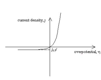
Figure 4.3.
Current density as function of overpotential for a semiconductor
Figure
4.4. Schematic distribution functions on the rate of electron transfer for a
semiconductor-solution interface
4.4. Highly doped semiconductors
When a semiconductor is
highly doped the Fermi level of the semiconductor may lie within the valence
band (VB) and the space charge region is very small. Electrons are able to
tunnel from the bulk of the valence band directly to the electrolyte. When this
occurs the semiconductor is said to be degenerately doped.
Considering the Frank-Condon
approximation to charge transfer at a degenerately doped electrode indicates
that electrons are transferred at or to energy levels close to the Fermi level.
As the concentration of
charge carriers available for exchange is constant (from the bulk) at a
degenerately doped electrode the current densities are:
ja µ (overlap of EF and ER)
jc µ - (overlap of EF and EO)
When the equilibrium
potential is reached the overlap integrals are identical. Hence ja ad jc are equal and the net current density is zero (by
definition jc is
negative).
When a positive
overpotential is applied
(overlap of EF and ER) > (overlap of EF
and EO)
then
ja < jc Þ j > 0
When a negative
overpotential is applied
(overlap
of EF and ER) < (overlap of EF and EO)
then
ja > jc Þ j < 0
Therefore these electrodes
show metal behaviour. This behaviour is shown in the schematic for figure 4.5.
Figure
4.5. Schematic distribution functions on the rate of electron transfer for a
heavily doped semiconductor-solution interface.
Current voltage curves
therefore resemble those at a metal, i.e., reduction and oxidation are found in
the plot, see figure 4.6.
Figure
4.6. Current density as a function of overpotential for a heavily doped
semiconductor.
4.4.1. Electrochemistry at Boron Doped Diamond Electrode
Many studies have been done
that report metal behaviour for boron doped diamond electrodes 6-41.
Two possible explanations
for metal behaviour on boron doped diamond are:
·
The
samples are degenerately doped.
·
Contamination
of the samples provides a conduction path through the films. Possible sources
of contamination are tantalum (Ta) from the filaments of the hot filament CVD
chamber and graphite (C) formed during the diamond growth.
These reasons can be
discounted as boron doped diamond displays:
·
A
Mott-Schottky regime 10, 42.
·
Two
time constants are measured in impedance experiments on boron doped diamond 10.
For an alternative explanation of the metallic behaviour on highly
doped diamond, the position of the conduction band minimum, the valence band
maximum, the energy of the surface states and the Fermi level relative to the
energy levels of the redox species in solution need to be considered.
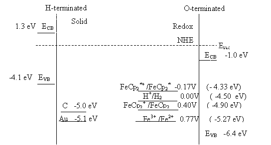
Figure 4.7. Schematic energy level diagram showing the band edges of the semiconductor and the energy levels of redox species 43. Redox potentials from CRC book 44.
For boron doped diamond the
surface termination needs to be considered:
·
Hydrogen
terminated diamond samples
·
Oxygen
terminated diamond samples
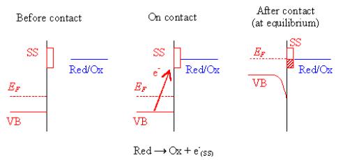
4.4.1.1. Hydrogen surface termination on highly doped diamond
For hydrogen terminated
diamond samples, the valence band maximum lies at higher energy than the proton
redox couple 10. In aqueous solution, holes will accumulate at the
surface.
A surface charge on the
semiconductor and the potential across the Helmholtz layer will result in the
material behaving in a metallic way. Figure 4.8 is a schematic of the contact
process between diamond and a standard hydrogen reaction as an example.
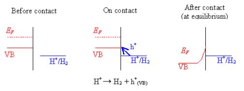
Figure 4.8. Reaction at a hydrogen terminated surface
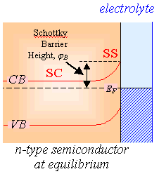
4.4.1.2. Oxygen terminated surface on highly doped diamond
The redox levels in solution
lie between the CB and VB. For a perfect single crystal diamond classic
semiconductor behaviour would be expected 42 . However, CVD polycrystalline doped diamond contains
a high density of grain boundaries. Grain boundaries are known to provide
trapping states 45, 46. The grain boundaries are graphitic in nature
suggesting they will lead to a density of surfaces states at an energy of
approximately –5.0 eV 2, 5(see figure 4.7). This energy level is comparable to
the energy levels of the redox couples in solution. To fully investigate the
role of the surface states in the mechanism requires a theory to describe in
detail the mechanism of surface state mediated charge transfer must be
developed.
Figure 4.9 shows a schematic
of the contact process for an oxygen terminated diamond surface, which includes
the surfaces states. The diagram explains a determinate situation when the
potential drop across the Helmholtz layer is constant.
Figure
4.9. Contact process for an oxygen terminated diamond surface (SS: surface
state)
4.5. Surface State Mediated Electron Transfer
Electron transfer via
surface states is often mentioned to explain some anomalies in semiconductor
electrochemistry 5.

Figure 4.10. Electron tranfer via surface states
In the literature little
information is available about the theory of charge transfer mediated by
surfaces states. Only Chazaviel et al.
47 and Vanmaekelbergh et al. 48, 49 consider the possibility of a charge transfer
mediated by surface states in an n-type semiconductor.
In this section the
Chazaviel model, which uses the Marcus-Gerischer theory, discussed above, will
be developed for a p-type semiconductor. The model assumes that the only pathway for electron transfer is a two step
process which involves the transfer between the redox system and the
semiconductor surface and the transfer between the semiconductor surface and
the semiconductor bulk. Another assumption is that the distribution function
for the surface states obeys Fermi statistics, even under nonequilibrium
conditions; in other words, the electrons in the surface states are thermalized
to lattice temperature, and only the position of their Fermi level can be
changed.
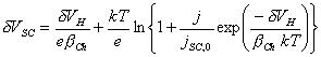
4.5.1. Contributions to the Applied Potential
The variation that the applied
potential experiences across a semiconductor electrode-solution interface, dV,
has two components: the potential difference across the space charge region in
the solid, dVSC, and the potential difference across the Helmholtz layer in the
solution, dVH.
dV =
dVSC + dVH [equation 4.3]
Here the importance of an
ohmic contact is apparent, it is required to avoid a potential drop across the
contact.
4.5.2 Contribution of the Helmholtz layer and the space charge region
The capacitance of the
Helmholtz layer, CH, is
assumed to be much bigger than that of the space charge region, CSC. This fact implies that
modifications in the potential drop across the Helmholtz layer, dVH, are only due to changes
in the surface charge dQ.
CSC << CH
![]()
[equation
4.4]
4.5.3. Electrical charge at the surface of semiconductor electrode
The change in the surface
charge is a function of the modification in the Fermi level energy at the
surface, E0, and the
density of the states at the surface, per unit of energy rSS.
![]()
[equation
4.5]
Reordering the above
equation:
![]() [equation
4.6]
[equation
4.6]
Substituting equation 4.6 in
equation 4.4 yield:
![]()
[equation
4.7]
Assuming that the
distribution of the surface states is uniform equation 4.7 is transformed to:
![]()
[equation
4.8]
Regrouping terms of the
equation:
![]()
[equation
4.9]
4.5.4. The Butler-Volmer Equation
Electron transfer across the Helmholtz layer is governed by the
Butler-Volmer equation 3.
In a non-equilibrium
situation, there is a difference in the energy between electrons in the surface
states and the redox couple. The Butler-Volmer equation relates the current
density to the potential drop across the Helmholtz layer.
Assuming efficient mass
transport:
![]() [equation 4.10]
[equation 4.10]
If a=0.5
![]() [equation 4.11]
[equation 4.11]
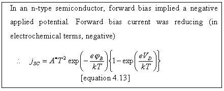
4.5.5. Schottky Diode.
The bulk
semiconductor-surface state junction may be modelled as a Schottky diode 50.
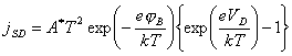
[equation 4.12]
Where jSD =
current across the space charge layer
VD = the potential drop between the space
charge and the
bulk semiconductor (the forward bias)
jB = barrier height
Figure 4.11 shows the
relationship between forward bias and conventional electrochemical current for
n-type and p-type semiconductors.
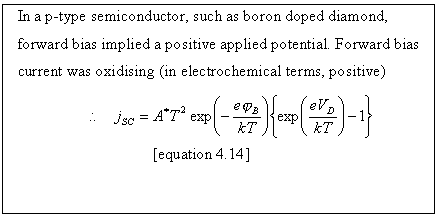
Figure
4.11. Forward bias and conventional electrochemical current. VD is the potential drop
between the semiconductor surface (SS) and the semiconductor bulk (SC).
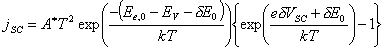
4.5.6. Model
Figure 4.12 below reflects
the influence of applying a positive potential to a semiconductor interface at
which there is a high density of surface states.
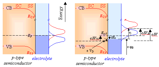
Figure 4.12. Schematic energetic diagram at positive potential
Expressions relating the
potential drop across each component can be obtained
![]()
[equation 4.15]
![]()
[equation 4.16]
![]()
[equation 4.17]
Substituting the expression
for the overpotential (equation 4.15) into
![]()
[equation 4.18]
yields:
![]() [equation 4.19]
[equation 4.19]
When the
semiconductor-surface state junction is considered as a Schottky-diode the
current across the space charge region is:
[equation 4.20]
Hence, the space charge
current across, jSC,0, at
equilibrium is:
[equation 4.21]
[equation 4.22]
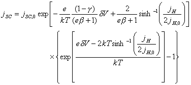
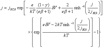
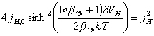
4.5.7. Steady State Current
When the steady state is
reached the net current density, j,
is equal to the current density in the Helmholtz layer and current density in
the space charge region.
jSC
= jH = j [equation 4.23]
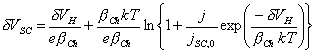
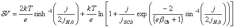
Substituting equation 4.9
into equation 4.19 gives:
 [equation 4.24]
Rewriting the above
equation, the expression for the applied potential in the Helmholtz layer
gives:
 [equation 4.25]
![]()
Substituting into equation 4.22:
 [equation 4.26]
Expanding the equation:
 [equation 4.27]
Applying the logarithmic
fuction:
 [equation 4.28]
Reorganizing the equation:
 [equation 4.29]
Simplyfying the above equation:
 [equation 4.30]
the applied potential in the
space charge region is obtained.
Substituing equation 4.3
into the equation 4.30 gives:
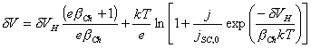
[equation 4.31]
for the net applied
potential.
Applying equation 4.25 to
the above equation:

[equation 4.32]
Considering that
![]() [equation 4.33]
[equation 4.33]
then
[equation 4.34]
Reorganizing the equation
[equation 4.35]
the net applied potential is
expressed in terms of the current density.
4.6. Developing the model
The model disscused in the
last section was a development of the theory of Chazalviel 47. It is based a the assumption that CH
>> CSC (see section 4.4.2.). A new model is required when this
supposition is not valid. The system must be modelled by accounting for the
potential drop across both the space charge region and the Helmholtz layer.
The space charge region and
the Helmholtz layer can be modelled as connected in series. Each region
performs as a resistor in parallel with a capacitor.
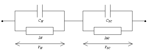
Figure 4.13. Equivalent circuit for surface mediated transfer with significant potential drop across the Helmholtz layer.
To describe the new model it
is necessary to calculate the relationship between current density and the
applied potential. Considering the above equivalent circuit and applying
Kirchoff’s laws:
![]() [equation 4.36]
[equation 4.36]
and
![]() [equation 4.37]
[equation 4.37]
Using equation 4.37 to
eliminate dVSC from
equation 4.36 yields:
![]()
[equation 4.38]
where QSS is the charge on the surface states.
If the density of surface
states per unit energy (eV) is rSS(E0)
![]() [equation 4.39]
[equation 4.39]
Hence:
 [equation 4.40]
or ![]() [equation 4.41]
[equation 4.41]
where  [equation 4.42]
If the capacitances, CH and CSC, and the density of states, r(E0), are potential independent the equations can be rewritten as:
![]() [equation 4.43]
[equation 4.43]
and
![]() [equation 4.44]
[equation 4.44]
Substituting equation 4.15
into equation 4.11 (the Butler-Volmer equation for a=0.5)
![]() [equation 4.19]
[equation 4.19]
Substituting 4.43 into 4.19
yields
![]() [equation 4.45]
[equation 4.45]
Regrouping terms yields
![]() [equation 4.46]
[equation 4.46]
Reordering the above
equation:
 [equation 4.47]
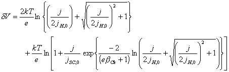
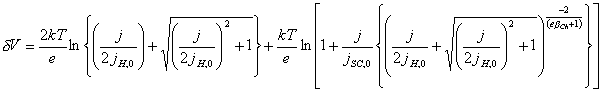
The current across the space
charge region, jSC can be
fitted as a Schottky diode (substitute equation 4.44) into the equation 4.22:
 [equation 4.48]
Substituting equation 4.47
into 4.48 yields:
[equation 4.49]
When the steady state is
reached, the stored charge is constant and the current through the Helmholtz
layer is equal that the space charge region
j = jH = jSC [equation 4.50]
Therefore, the equation 4.50
can be rewritten:
[equation 4.51]
Equation 4.51 is an
expression for the current density, j,
that modifies with the applied overpotential, dV. The rest of the terms are
constant. No analytical solution to the equation can be obtained and numerical
methods are necessary required then.
Mathcad 8 Profesional
(MathSoft, Inc.) was operated to find numerical solutions. The software could
automatically select an appropriate algorithm to solve a given equation. The
solutions found by numerical means were not necessarily unique.
It is usual in semiconductor
electrochemistry to suppose that the capacitance of the Helmholtz layer to be
much bigger than that of the space charge region (CH>>CSC). If that is the case, then g tends to unity (g®1) and the equation can be
solved analytically.
When g=1, then equation 4.51 simplifies to equation
4.32:
[equation 4.32]
i.e.
the general model obtains the particular case of the Chazaviel model, when g®1.
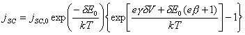
4.6.1. The case when ½jH,0½>>½j½
For the case when ½jH,0½>>½j½, several terms in equation
4.51 become negligible. This leads to much simpler relationship shows in the
equation 4.52.
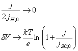 [equation 4.52]
Figure 4.14 shows a Mathcad plot for the equation 4.51 when ½jH,0½>>½j½. The behaviour is
independent of b and is typical of a p-type
semiconductor.

Figure
4.14. Equation 4.51 plotted for |jH,0|>>|j|.
From the figure 4.14 it can be deduced that when ½jH,0½>>½j½, ideal semiconductor behaviour is expected for boron doped diamond. Such behaviour is not reached in the experimental conditions. Factors like the diffusion of the electrolyte (or redox couple), possible chemical reaction on the surface, etc avoid an ideal semiconducting behaviour. Thefore the figure 4.14 represents a boundary situation.
4.6.2. The case when ½j½>>½jH,0½
When ½j½>>½jH,0½,
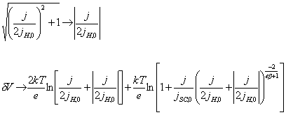 [equation 4.53]
For positive j:
 [equation 4.54]
For negative j:
![]() [equation 4.55]
[equation 4.55]
When negative potentials are
applied, the current density is independent of the applied potential.
Figures 4.15 show Mathcad
plot of equation 4.51 for the case when ½j½>>½jH,0½. The behaviour is
independent of b and is typical of a p-type
semiconductor.
Figure
4.15. Equation 4.51 plotted for |jH,0|<<|j|.
Figures 4.15 suggests an
ideal semiconductor behaviour for boron doped diamond when ½j½>>½jH,0½. Diffussion effects,
possible chemical reactions on the electrode surface, etc. can contribute in the deviation of the results obtained in
experimental conditions from the situation expressed in the figure 4.15.
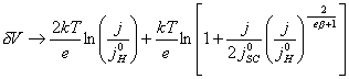
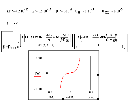
4.6.3. The case when ½jSC,0½>>½j½ and j» jH,0
For the case when ½jSC,0½>>½j½ and j» jH,0, equation 4.51 simplifies
to equation
4.56.
 [equation 4.56]
Figure 4.16 shows a Mathcad
plot equation 4.51 for the case when ½jSC,0½>>½j½. The behaviour is
independent of b and is classic metal
behaviour.

Figure 4.16. Equation 4.51 plotted for |jSC,0|>>|j|.
Figure 4.16 shows the
standard metal behaviour for boron doped diamond. In these conditions surface states promote the electron transfer in
such as way that metal behaviour is obtained.
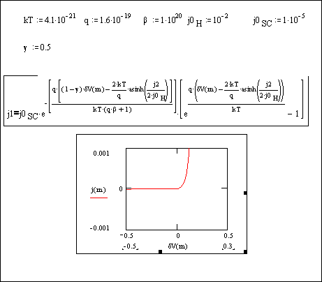
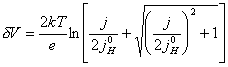
4.6.4. Considering doping levels
When high doping levels are
reached, jSC,0 values are
high. Metal behaviour is observed. Reducing the doping level, implies that jSC,0 becomes more important
and semiconductor behaviour is observed.
Figures 4.17 and 4.18 show Mathcad
plots of equation 4.51 for different values of b and the rest of parameters equal.
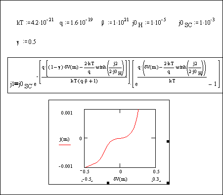
Figure 4.17. Equation 4.51 plotted
for |jSC,0|>|j| and b=1´1021.
Figure
4.18. Equation 4.51 plotted for |jSC,0|>|j|
and b=1´1024.
Figure 4.17 shows a intermediate situation between
metal behaviour and ideal behaviour for boron doped diamond. It behaves as
semiconductor (electron transfer is not as easy as in a metal) but it shows a
maximum for a region of the curve, typical of a metal behaviour. Figure 4.17 shows the typical behaviour in
experimental conditions for a low doped diamond sample (see chapter 5).
Figure 4.18 shows metal behaviour. When the doping
level is increased boron doped diamond behaves as a metal.
Summarising at this point, semiconductor behaviour
will be observed for boron doped diamond if the total current density values
are different enough from the values of Helmholtz current density values. In
case that the total current density values are similar to the Helmholtz ones
space charge current density plays an important role. When the magnitude of the
space charge current density is much bigger than the one for the total current
density, just only in this case, metal behaviour will be observed. Otherwise
semiconductor behaviour remains.
4.7. AC
Impedance
The surface state model can be extended to consider
small amplitude modulations (symbolised by overtilde embellishments). To
facilitate the mathematical development is considered that CH>>CSC,
in other words that g»1
![]() [equation 4.57]
[equation 4.57]
Applying Kirchoff’s law:
![]() [equation 4.58]
[equation 4.58]
![]() [equation 4.59]
[equation 4.59]
Using the general equation for the current density
across Helmholtz layer
![]()
[equation 4.19]
using ![]() equation above becomes
equation above becomes
 [equation 4.60]
and applying small perturbations yields:
 [equation 4.61]
Expanding
the above equation using ![]()
[equation 4.62]
As
[equation 4.63]
and
[equation 4.64]
The equation 4.62 is simplified to:
 [equation 4.65]
A further simplification can be done if
![]()
[equation 4.19]
leaving the equation 4.65 as:
 [equation 4.66]
Rewriting the above equation as
 [equation 4.67]
and considering ![]()
 [equation 4.68]
As
 [equation 4.69]
then the equation 4.68 yields:
![]() [equation 4.70]
[equation 4.70]
If ![]() the equation 4.70
becomes:
the equation 4.70
becomes:
![]() [equation 4.71]
[equation 4.71]
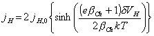
The current density of the space charge layer using
Chazaviel model for a p-type semiconductor is expressed
 [equation 4.72]
substituting equation 4.3 into the above equation
yields

[equation 4.73]
Applying small perturbations yields

[equation 4.74]
Expanding the above equation
[equation 4.75]
Substituting in the small perturbation terms for exp(x) »1 + x and exp(y) »1 + y
![]()
[equation 4.76]
Considering that x
´ y ® 0 the above equation yields:
[equation 4.77]
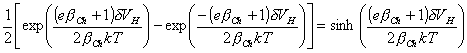
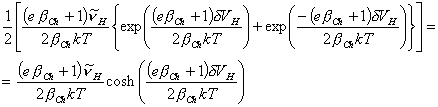
Regrouping terms using equation 4.73 yields
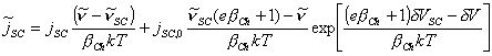
[equation 4.78]
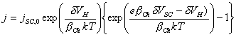
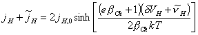
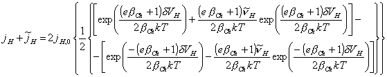
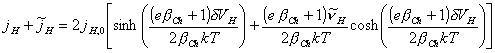
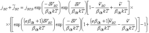
For steady DC current, j=jSC
![]() and
and  then equation 4.78
becomes:
then equation 4.78
becomes:
![]() [equation 4.79]
[equation 4.79]
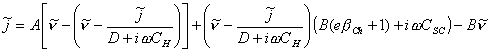
For a particular potential, j, bCh, jH,0 and dVSC remain constant. dV, dVSC and j can be determined from
steady-state measurements.
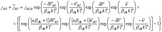
Equations 4.57,4.58,4.59,4.71, and 4.77 can be
combined to lead to an expression which eliminates ![]() and
and ![]() .
.
Substituting the equation 4.71 into the equation
4.58 yields:
![]() [equation 4.80]
[equation 4.80]
and substituting the equation 4.79 into the equation
4.59 gives:
![]() [equation 4.81]
[equation 4.81]
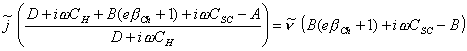
Substituting the equation 4.57 into the equation
4.80
![]() [equation 4.82]
[equation 4.82]
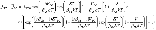
Rewriting the above equation
![]() [equation 4.83]
[equation 4.83]
Substituting the equation 4.83 into the equation
4.81 gives:
[equation 4.84]
Expanding the above equation:
[equation 4.85]
![]() [equation 4.86]
[equation 4.86]
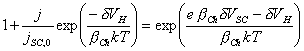
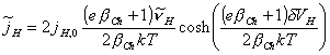
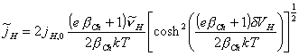
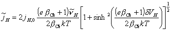
Therefore impedance is
![]() [equation 4.87]
[equation 4.87]
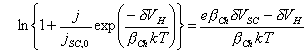
Considering the case when j=0 (at open circuit potential conditions), the expression in the
equation 4.87 simplifies to:
![]() [equation 4.88]
[equation 4.88]
If ebCh >>1 (metal behaviour
for highly boron doped diamond electrode) equation 4.88 becomes
![]() [equation 4.89]
[equation 4.89]
This expression for Z forms two semicircles when
plotted in the complex plane. The first semicircle has a radius of 1/BebCh with a maximum, wmax, of BebCh /CSC. The second semicircle has a radius
of 1/D and a maximum, wmax, of D/CH.
This theory fits the experimental results found for several research groups10, 42, 51-53.
When the conditions are not at open circuit
potential, the behaviour is slightly more complicated and it is necessary to
find values of j, dV
and dVSC from DC experiments.
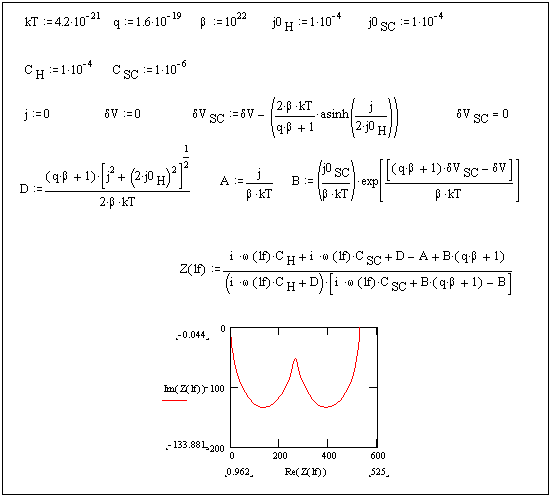
Figure 4.19. Impedance plot for open circuit potential conditions
Figure 4.19 shows two semicircles at open circuit potential conditions. This behaviour has been reported frequently for highly boron doped diamond electrodes 10, 42.
In the effort to characterise properly the semiconducting behaviour of boron doped diamond the semicircle generated for the capacitance of the space charge layer (in the impedance plot) requires to be studied in detail. For this purpose the Mott Schottky equation (see chapter 5) relates the space charge capacitance per unit area and the potential of the surface with respect to the bulk semiconductor. In chapter 5 Mott Schottky plots are used to characterise the semiconducting properties of moderately boron doped polycrystalline diamond.
4.8. Summary
The standard theories for metal or semiconductor electrochemistry
are outlined. The models do not agree
with the electrochemistry of boron doped polycrystalline diamond films,
reported in the literature.
The mechanism of charge transfer must be considered.
The presence of a surface explains the difference in behaviour between hydrogen
and oxygen terminated diamond films.
A relationship between the current density and
applied potential has been derived. This agrees with the experimental results
of these research groups 25-31,
33, 36, 37, 39-41, 54-65, which show metallic behaviour. The theory suggests
that at low doping levels semiconductor behaviour may be observed.
The surface state model was applied to the AC
impedance studies and an expression was deduced that predicts the two time constants
that have been observed for several groups.
The results from the AC impedance have been linked
to the Mott Shottky equation to investigate the capacitance associated with the
space charge layer that defines the semiconducting properties for boron doped
diamond.
4.9.
References
1 R. A. Marcus, J. Chem. Phys., 1965, 43, 679.
2 S. R. Morrison,
'Electrochemistry at Semiconductor and
Oxidized Metal Electrodes', Plenum Press, 1980.
3 A. C. Fischer, 'Electrode
Dynamics', Oxford University Press, 1996.
4 P. Atkins, 'Physical
Chemistry', Oxford University Press, 1994.
5 A. J. Bard and L. R.
Faulkner, 'Electrochemical Methods Fundamentals and Applications', 2001.
6 F. J. Del Campo, C. H.
Goeting, D. Morris, J. S. Foord, A. Neudeck, R. G. Compton, and F. Marken, Electrochem. Solid State Lett., 2000, 3, 224.
7 S. Ferro, A. De Battisti, I.
Duo, C. Comninellis, W. Haenni, and A. Perret, J. Electrochem. Soc., 2000, 147,
2614.
8 D. Gandini, E. Mahe, P. A.
Michaud, W. Haenni, A. Perret, and C. Comninellis, J. Appl. Electrochem., 2000, 30,
1345.
9 C. H. Goeting, F. Marken, A.
Gutierrez-Sosa, R. G. Compton, and J. S. Foord, Diam. Relat. Mater., 2000, 9,
390.
10 M. N. Latto, D. J. Riley,
and P. W. May, Diam. Relat. Mater.,
2000, 9, 1181.
11 P. A. Michaud, E. Mahe, W.
Haenni, A. Perret, and C. Comninellis, Electrochem.
Solid State Lett., 2000, 3, 77.
12 H. Notsu, I. Yagi, T.
Tatsuma, D. A. Tryk, and A. Fujishima, J.
Electroanal. Chem., 2000, 492,
31.
13 Y. V. Pleskov, V. M. Mazin,
Y. E. Evstefeeva, V. P. Varnin, I. G. Teremetskaya, and V. A. Laptev, Electrochem. Solid State Lett., 2000, 3, 141.
14 T. N. Rao and A. Fujishima, Diam. Relat. Mater., 2000, 9, 384.
15 T. N. Rao, B. V. Sarada, D.
A. Tryk, and A. Fujishima, J.
Electroanal. Chem., 2000, 491, 175.
16 B. V. Sarada, T. N. Rao, D.
A. Tryk, and A. Fujishima, Anal. Chem.,
2000, 72, 1632.
17 A. J. Saterlay, S. J.
Wilkins, C. H. Goeting, J. S. Foord, R. G. Compton, and F. Marken, J. Solid State Electrochem., 2000, 4, 383.
18 O. Chailapakul, P. Aksharanandana,
T. Frelink, Y. Einaga, and A. Fujishima, Sensors
and Actuators B-Chemical, 2001, 80,
193.
19 J. S. Foord, K. B. Holt, R.
G. Compton, F. Marken, and D. H. Kim, Diam.
Relat. Mater., 2001, 10, 662.
20 A. Fujishima and T. N. Rao, Diam. Relat. Mater., 2001, 10, 1799.
21 P. L. Hagans, P. M.
Natishan, B. R. Stoner, and W. E. O'Grady, J.
Electrochem. Soc., 2001, 148,
E298.
22 K. B. Holt, J. Del Campo, J.
S. Foord, R. G. Compton, and F. Marken, J.
Electroanal. Chem., 2001, 513,
94.
23 F. Marken, Y. C. Tsai, A. J.
Saterlay, B. A. Coles, D. Tibbetts, K. Holt, C. H. Goeting, J. S. Foord, and R.
G. Compton, J. Solid State Electrochem.,
2001, 5, 313.
24 F. Marken, R. G. Compton, C.
H. Goeting, J. S. Foord, S. D. Bull, and S. G. Davies, J. Solid State Electrochem., 2001, 5, 88.
25 H. Notsu, T. Fukazawa, T.
Tatsuma, D. A. Tryk, and A. Fujishima, Electrochem.
Solid State Lett., 2001, 4, H1.
26 M. Panizza, P. A. Michaud,
G. Cerisola, and C. Comninellis, J.
Electroanal. Chem., 2001, 507,
206.
27 M. Panizza, P. A. Michaud,
G. Cerisola, and C. Comninellis, Electrochem.
Commun., 2001, 3, 336.
28 A. J. Saterlay, S. J.
Wilkins, K. B. Holt, J. S. Foord, R. G. Compton, and F. Marken, J. Electrochem. Soc., 2001, 148, E66.
29 N. Spataru, T. N. Rao, D. A.
Tryk, and A. Fujishima, J. Electrochem.
Soc., 2001, 148, E112.
30 N. Spataru, B. V. Sarada, E.
Popa, D. A. Tryk, and A. Fujishima, Anal.
Chem., 2001, 73, 514.
31 D. A. Tryk, K. Tsunozaki, T.
N. Rao, and A. Fujishima, Diam. Relat.
Mater., 2001, 10, 1804.
32 Y. C. Tsai, B. A. Coles, K.
Holt, J. S. Foord, F. Marken, and R. G. Compton, Electroanalysis, 2001, 13,
831.
33 R. Uchikado, T. N. Rao, D.
A. Tryk, and A. Fujishima, Chem. Lett.,
2001, 144.
34 J. D. Wadhawan, F. J. Del
Campo, R. G. Compton, J. S. Foord, F. Marken, S. D. Bull, S. G. Davies, D. J.
Walton, and S. Ryley, J. Electroanal.
Chem., 2001, 507, 135.
35 W. L. Wang, K. J. Liao, R.
Q. Zhang, and C. Y. Kong, Materials
Science and Engineering B-Solid State Materials for Advanced Technology,
2001, 85, 169.
36 J. Lee, D. A. Tryk, A.
Fujishima, and S. M. Park, Chem. Commun.,
2002, 486.
37 A. Manivannan, M. S. Seehra,
D. A. Tryk, and A. Fujishima, Anal. Lett.,
2002, 35, 355.
38 K. Ohnishi, Y. Einaga, H.
Notsu, C. Terashima, T. N. Rao, S. G. Park, and A. Fujishima, Electrochem. Solid State Lett., 2002, 5, D1.
39 C. Prado, G. U. Flechsig, P.
Grundler, J. S. Foord, F. Marken, and R. G. Compton, Analyst, 2002, 127, 329.
40 T. N. Rao, B. H. Loo, B. V.
Sarada, C. Terashima, and A. Fujishima, Anal.
Chem., 2002, 74, 1578.
41 C. Terashima, T. N. Rao, B.
V. Sarada, D. A. Tryk, and A. Fujishima, Anal.
Chem., 2002, 74, 895.
42 J. van de Lagemaat, D.
Vanmaekelbergh, and J. J. Kelly, J.
Electroanal. Chem., 1999, 475,
139.
43 G. Pastor-Moreno and D. J.
Riley, Electrochim. Acta, 2002, 47, 2589.
44 D. R. Lide, in 'CRC Handbook
of Chemistry and Physics', ed. D. R. Lide, 1994.
45 T. N. Rao, D. A. Tryk, K.
Hashimoto, and A. Fujishima, J.
Electrochem. Soc., 1999, 146,
680.
46 S. Nakabayashi, N. Ohta, and
A. Fujishima, PCCP, 1999, 1, 3993.
47 J. N. Chazalviel, J. Electrochem. Soc, 1982, 129, 923.
48 D. Vanmaekelbergh, Electrochim. Acta, 1997, 42, 1135.
49 D. Vanmaekelbergh, Electrochim. Acta, 1997, 42, 1121.
50 S. M. Sze, 'Semiconductor
devices, physics and technology', ed. J. Wiley, 1985.
51 G. M. Swain, J. Electrochem. Soc., 1994, 141, 3382.
52 R. Ramesham and M. F. Rose, Diam. Relat. Mater., 1997, 6, 17.
53 S. Yoshihara, K. Shinozaki,
T. Zenbayashi, S. Morino, T. Shirakashi, K. Hashimoto, D. A. Tryk, and A.
Fujishima, Electrochim. Acta, 2000, 45, 3375.
54 R. F. Mamin and T. Inushima,
Synthetic Metals, 2001, 121, 1219.
55 R. F. Mamin and T. Inushima,
Physical Review B, 2001, 6303, art. no.
56 C. E. Nebel, R. Zeisel, and
M. Stutzmann, Diam. Relat. Mater.,
2001, 10, 639.
57 M. A. Rodrigo, P. A.
Michaud, I. Duo, M. Panizza, G. Cerisola, and C. Comninellis, J. Electrochem. Soc., 2001, 148, D60.
58 A. J. Saterlay, J. S. Foord,
and R. G. Compton, Electroanalysis,
2001, 13, 1065.
59 J. M. Stotter, S. Haymond,
J. E. Butler, G. M. Swain, and J. K. Zak, Abstracts
of Papers of the American Chemical Society, 2001, 222, 117.
60 M. A. Witek and G. M. Swain,
Abstracts of Papers of the American
Chemical Society, 2001, 222, 59.
61 M. A. Witek and G. M. Swain,
Anal. Chim. Acta, 2001, 440, 119.
62 F. Marken, C. P. Paddon, and
D. Asogan, Electrochem. Commun.,
2002, 4, 62.
63 G. Pastor-Moreno and D. J.
Riley, Electrochem. Commun., 2002, 4, 218.
64 C. Prado, S. J. Wilkins, F.
Marken, and R. G. Compton, Electroanalysis,
2002, 14, 262.
65 I. Yagi, K. Tsunozaki, A.
Fujishima, B. Ohtani, and K. Uosaki, J.
Electrochem. Soc., 2002, 149,
E1.