Chapter 2
Growth and Characterisation of the Diamond Films
2.0 Outline
·
This
chapter describes the diamond growth method used in this study and explains why
it was chosen.
·
The
main components of the diamond growth apparatus are described.
·
The
benefits of four different types of electrical contact are compared.
·
Scanning
electron microscopy, optical microscopy and Raman spectroscopy were used to
characterise the films and the results are presented here.
2.1 The Choice of Growth
Technique
Hot filament chemical vapour
deposition (HFCVD) was used to grow diamond films for these studies. HFCVD
diamond was first produced in 1952. 61,62 The technique is now
established and has been well described in a number of review articles. 11,17,18
Extensive work has previously been performed on similar HFCVD set-ups at the
University of Bristol. 63-65
The chemical vapour
deposition (CVD) process had a combination of properties that made it the
method of choice for fabricating the diamond films in this study:
·
The
use of gaseous reagents was easily controlled and allowed the composition of
the reaction mixtures to be varied.
·
The
technique produces continuous films which, if grown on planar substrates, were
macroscopically flat. These films were ideal for use as planar electrodes. The
technique could also be extended to coat metal wires with diamond, 66 which could be used in a range of
alternative electrode geometries. 67
·
Diamond
films were produced which covered a surface area of several square centimetres.
While certain other techniques could coat significantly larger areas, much work
on the electrochemistry of diamond had previously studied smaller single
crystal diamonds and homoepitaxial layers grown onto single crystals. The
larger surface area available with CVD diamond allowed for a range of
electrodes to be fabricated that were ideal for laboratory experiments.
HFCVD was used in preference
to more sophisticated forms of CVD for a variety of reasons:
·
The
apparatus was sufficiently simple to allow thorough cleaning of the inside of
the reaction chamber. This was necessary to remove boron contamination.
·
The
relative simplicity of the design allowed for modifications to the chamber to
be introduced as required.
·
The
components necessary to assemble a HFCVD chamber are relatively inexpensive.
·
The
HFCVD technique has been studied extensively and there is a reasonable
understanding of the processes involved. The growth apparatus used in this
study was a modified version of a well characterised HFCVD chamber and this
significantly reduced the work necessary to characterise and optimise the
growth conditions.
The use of HFCVD applied a
number of restrictions on work that could be performed:
·
HFCVD
does not give the high rates of growth available from certain other techniques,
such as plasma torches, 19,68 and so thick films could not be grown.
If sufficiently thick diamond films had been grown then the silicon substrate
could have been etched away in a bath of hydrofluoric acid (HF) and nitric acid
(HNO3). 69 This
would have left a free-standing diamond film which can be used in a range of
applications.
·
The
use of hot-filament CVD prevented the use of any oxygen containing gas species.
The presence of species such as oxygen (O2), carbon monoxide (CO),
carbon dioxide (CO2), trimethylborate (TMB, B(OCH3)3)
or water (H2O) would have caused the rapid burn out of the tantalum
(Ta) filaments.
·
Metallic
contamination of the diamond films from the filament was a potential problem.
The possibility of surface or bulk tantalum (Ta) affecting the electrochemical
or electrical properties had to be considered. 70,71 Any possible
effect of tantalum could be reduced if the diamond films were treated in acids
before use. Refluxing in hot nitric acid could be used to remove any graphitic
(sp2) content in the surface layer of the films and a short (ten
second) dip in warm chromic acid (H2Cr2O7) † could be used to oxidise the surface of
the films.
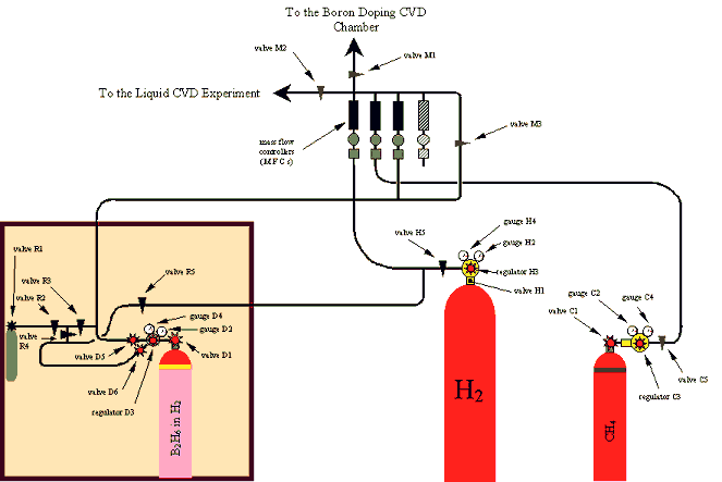
Figure 2.1 - A schematic diagram of the gas lines which fed the diamond CVD chamber
2.2 The Reaction Gases
Figure 2.1 shows a schematic
diagram of the experimental set-up of the gas lines which fed the reaction
chamber.
Hydrogen (H2),
methane (CH4) and diborane (B2H6) gases (BOC
Speciality Gases) were used in the growth process. See section 2.10 for details
of the reaction conditions.
Laboratory standard “high
purity hydrogen” and methane were used. The purities of the hydrogen and
methane were 99.995% (“N4.5”) and 99.5% (“N2.5”) respectively.
Diborane was chosen as the
boron source because it held advantages over most other sources. Table 2.1
summarises these advantages and disadvantages of commonly used sources.
|
Boron Source |
Formula |
Advantages |
Disadvantages |
References |
|
diborane |
B2H6 |
· simple
molecular chemistry · gas source provides excellent controllability and variability of concentrations · availability† |
· highly toxic · highly explosive · highly reactive |
72 - 75 |
|
trimethyborate (TMB) |
B(OCH3)3 |
· non-toxic |
· liquid source requires dilution in acetone (CH3)2CO or methanol CH3OH |
78 - 84 |
|
boron (rod or powder) |
B |
· solid added directly to chamber - easy to store |
· lack of controllability and variability of concentration |
67, 85, 86 |
|
boron trioxide |
B2O3 |
· readily available |
· solid source requires dissolution in acetone (CH3)2CO or methanol CH3OH‡ |
87 - 91 |
|
ex-situ ion implantation |
B+ |
· can dope any diamond sample · good controllability · achieve low doping levels |
· non-uniform doping profile · damage to diamond sample due to high energy bombardment |
93 |
Table 2.1
A summary of the advantages
and disadvantages of various boron sources
The diborane was a special
order gas which was supplied as a 4.75% premix of diborane in hydrogen.
Diborane is a highly explosive, toxic and reactive gas. Great care was taken to
ensure that all gas lines were leak tested before use. The gas cylinder, the
dilution cylinder and the associated piping were housed in a specially designed
fume cupboard to provide some secondary protection in the event of an accident.
The reactivity of diborane made it necessary to avoid the use of many materials
including brass and nitrile rubber.
The source gases were stored
in gas cylinders with nominal pressures up to 200 bar at 15 °C.
Regulators reduced the cylinder pressures to the level of one to two bar above
atmospheric pressure. Mass flow controllers then set the flow rates into a gas
manifold where the gases mixed before they flowed along a common gas line into
the reaction chamber.
The regulator on the
diborane gas cylinder was a stainless steel single stage design which could be
pumped down to vacuum and contained a purge line. This also allowed the
dilution procedure to be performed (see section 2.4). The hydrogen and methane
gas cylinders used standard single stage brass regulators.
Low levels of impurities in
the hydrogen gas could be significant because of the relative flow rates of the
source gases. A typical gas mixture may use as many as seven orders of
magnitude more hydrogen than diborane. Therefore an impurity species in the
hydrogen with a concentration of only one hundred thousandth of one percent
(0.00001%) would have a concentration in the mixture of gases comparable to
that of the diborane present. Fortunately, nitrogen (N2), the main
impurity present, did not effect the growth process or the electrical
characteristics of the diamond films. Nitrogen is not incorporated into diamond
during growth as rapidly as boron 94 and it tends to occupy
electrically inactive sites. 95-97 The effects of nitrogen on the
growth rate and surface morphology of the diamond also require higher
concentrations than present in the reaction mixture. 98-99
2.3 The Mass Flow
Controllers
A bank of three mass flow
controllers (MFCs) was used to set the flow rates of the gases. Each MFC
controlled the flow of gas through a gas line and into a manifold where the
gases were mixed. The MFCs were manufactured by Tylan General and their
specifications are detailed in Table 2.2.
The MFCs were controlled
electronically and could be adjusted to give a wide range of flow rates. They
performed less well if the rate of flow was reduced below five percent of the
maximum flow rate and so alternative methods was needed to obtain low flow
rates. For this reason, the diborane MFC was replaced with a lower capacity
model when boron doping levels below 3000 p.p.m. were to be achieved.
The MFCs could be set to
115% of their nominal maximum flow rate to enable rapid pumping down of the
system. However, this was not sufficient to allow the diborane line to be
pumped down in a reasonable time and so a bypass valve was fitted beside the
MFC. The diborane MFCs used viton seals and were compatible with the gas.
|
MFC number |
Gas |
Calibration |
Range (s.c.c.m.) |
Conversion |
|
|||||
|
1 |
Hydrogen (H2) |
Hydrogen |
0 - 200 |
1 |
|
|||||
|
2 |
Methane (CH4) |
Nitrogen |
0.0 - 10.0 |
0.72 |
|
|||||
|
3 |
Diborane (B2H6) |
Hydrogen |
0.0 - 10.0 |
1 |
|
|||||
|
4 |
not used |
|
|
|
|||||
Table 2.2 - Specifications
of the Mass Flow Controllers
A fourth MFC was available
to allow more gases to be added to the reaction mixture. This facility was not
used in this study. However, it has been proposed that adding hydrogen sulphide
(H2S) or ammonia (NH4) would enable co-doping of the
diamond film with sulphur (S) or nitrogen (N) respectively.
The mixing manifold had a
second output to allow the MFCs to be used to supply other experiments with
hydrogen or methane when the CVD chamber was not running. In particular, the
hydrogen line was used to supply a prototype liquid CVD reactor.
2.4 Dilution of the Diborane
Gas
The diborane gas was
supplied pre-mixed with hydrogen. The nominal concentration was five percent
diborane in hydrogen. This proved far too concentrated for the deposition of
low doped diamond films and so a dilution system was constructed which allowed
the premix to be further diluted with hydrogen. This process could be performed
a number of times to allow the levels of diborane in the reaction mixture to be
reduced by several orders of magnitude. A lecture bottle with a capacity of 0.4
litres was used as a mixing vessel. Once the diborane was diluted, the lecture
bottle acted as a reservoir which could supply gas for approximately twenty
hours at a typical flow rate equivalent to 4 × 10⁻⁵ s.c.c.m.
of pure diborane. A photograph of the dilution assembly is shown in figure 2.2.
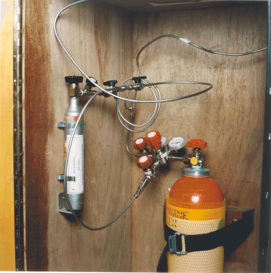
Figure
2.2 -A photograph of the diborane dilution assembly
The dilution method was a
highly effective technique for obtaining low concentrations of diborane but it
added significantly to the error in the measurement. The pressures used in the
dilution procedure were read from the pressure gauge on the diborane regulator.
This was not sufficiently sensitive to give a highly precise reading and so the
random errors were significant. The calculation below shows the effect of a
triple dilution on the error in the measurement of diborane concentration. The
physical displacement of the gauge from the lecture bottle also gave rise to
the possibility of a systematic error.
The calculation below shows
the random error for a triple diborane dilution and using a formula given in
reference 100. The errors used for the readings are half a scale division.
Typical values for a triple diborane dilution:
molar fraction of diborane in premix, R = (0.0475 ± 0.00005)
pressure of first fill of diborane mixture, pD1
= (0.500 ± 0.125) bar
pressure of first fill of hydrogen dilutant, pH1
= (2.6 ± 0.1) bar
pressure of second fill of diborane mixture, pD2
= (0.500 ± 0.125) bar
pressure of second fill of hydrogen dilutant, pH2
= (2.6 ± 0.1) bar
pressure of third fill of diborane mixture, pD3
= (0.500 ± 0.125) bar
pressure of third fill of hydrogen dilutant, pH3
= (2.6 ± 0.1) bar
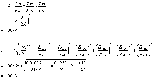
molar fraction of
fully diluted diborane = r
\ molar fraction of fully diluted diborane, r = 0.0034 ± 0.0006
The random error in the
measurement of the gas phase composition can be up to nineteen percent.
2.5 The Deposition Chamber
A photograph of the
deposition chamber is shown in figure 2.3.
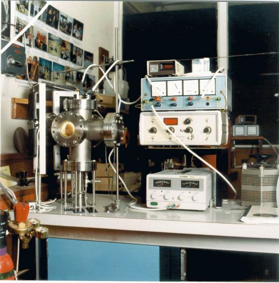
Figure
2.3 -A photograph of the deposition chamber
The deposition chamber
consisted of a single-walled stainless steel six-way cross with welded joints
and bolted flanges.
The top flange incorporated
three pairs of electrical contacts made from tungsten (W) rods. Glass coatings
were used to electrically insulate the rods as they fed through the flange.
Vacuum seals were made with epoxy resin and silicone rubber. One pair of
contacts was used to supply power to the substrate heater and the other two
supplied power to the filaments. The deposition chamber was electrically
earthed by a cable attached to the top flange. The casing of the rotary pump
provided a second route to ground.
The front flange housed a
glass window which provided a viewing port to allow for visual inspection of
the reaction. The window also allowed for measurement of the temperature of the
hot filament using an optical pyrometer.
Three gas lines fed into the
reaction chamber via the rear flange: the reaction gas inlet leading from the
mixing manifold; a connection to a capacitance diaphragm pressure gauge
(Baratron) which was used to measure the pressure in the chamber during diamond
growth runs; and an air vent valve which allowed the chamber to be brought up
to atmospheric pressure before it was opened.
The bottom flange led to a
two-stage rotary pump via two stainless steel gas lines. A large bore line,
with an internal diameter (int. Æ) of approximately
20 mm, allowed the vacuum system to be pumped down rapidly. A narrow bore
line, int. Æ 3 mm, fitted with a needle
valve allowed for greater control of pressure required for diamond deposition.
The openings to both these lines were protected from debris by a copper (Cu)
gauze. The exhaust line from the rotary pump was safely routed to an outlet on
the roof of the building.
The flange on the left-hand
side of the chamber was blank while the right-hand one incorporated a spare
pair of electrical feed-throughs.
The top flange could be
readily removed for access to the chamber. The filament holders and substrate
heater assembly were attached to the underside of this flange, to allow the new
filaments to be fitted and the substrates to be loaded before the assembly was
loaded into the deposition chamber.
The other flanges could be
removed to allow for thorough cleaning of the system. This was required
whenever the level of boron contamination became too high to maintain
reproducible levels of doping in the diamond films. In practice, this procedure
was performed when the required boron doping level in the diamond films was
reduced significantly.
During operation, the
deposition chamber was air cooled by four fans.
2.6 The Substrate Heater
A substrate heater was made
from a coil of nichrome wire [nickel-chromium (Ni‑Cr) 24 SWG, standard
wire gauge]. The wire was threaded through insulating ceramic beads and then
coiled. The coil of wire was then encased in fire cement and gently heated to
allow the cement to set. It was important to drive off any water that could be
released into the chamber in order to prevent oxidation of the hot filaments. A
molybdenum (Mo) plate was placed onto the top of the cement block to provide a
flat surface on which the substrates could be placed. Molybdenum was chosen
because it has a high melting point, it is inert under the reaction conditions
and is effective in evenly spreading the heat to the base of the substrates.
The substrate heaters were
operated by passing a current of 4 A through the nichrome wire. A potential of
15 to 20 V was required to achieve this current depending on the length of wire
used in the construction of the heater. From previous studies on similar
systems, it is estimated that the hot filaments reached 2400 °C and provided
additional radiative heating which raised the substrate temperature to 900 °C. 64
The maximum operating temperature of the substrate heater was limited by the
breakdown of the fire cement at approximately 1000°C which would cause water
vapour to be released into the chamber and lead to burn out of the filaments.
The substrate heaters had an
operational lifetime in the order of eight hundred hours, after which the
resistance wires would become too brittle and break. This allowed for
approximately ninety growth runs during the life of the heater. The periodic
replacement of the heater was also important to reduce residual boron levels in
the chamber as the heating block could not be cleaned and the fire cement was
believed to be a significant source of contamination due to its porous nature.
Electrical connections
between the heating block and the tungsten feed-throughs were made with standard
copper flex insulated by ceramic beads.
An Iso-tech DC power supply
was used for the substrate heater and this was protected from overheating by an
external fan behind the heat exchanger at the rear of the unit.
2.7 The Filaments
The CVD reactor used
tantalum (Ta) filaments which were prepared by coiling a length of wire around
a 4 mm rod. The shaft of a screwdriver was routinely used for this purpose. The
wire used had a diameter of 0.25 mm. Previous work by the group had used
six-turns of wire which spanned approximately one centimetre. The chamber used
for this study was designed for larger scale deposition. It was found that ten
turns of wire spanning 2 cm was the optimum scale for the system as longer
filaments tended to sag during operation which resulted in poor diamond growth.
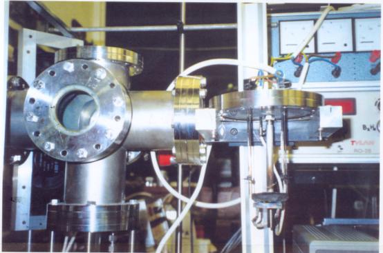
Figure 2.4
- A photograph of the deposition chamber showing the
internal
assembly after a deposition run - the heating stage and
a
drooping tantalum filament are visible
Previous studies had used
single filament set-ups. The chamber used for this experiment was a double
filament arrangement. This allowed for either a larger deposition area to be
covered or for two or more substrates to be coated simultaneously. The two
filaments were connected in series with the connection being made outside the
chamber. The apparatus could be readily reconfigured to allow single filament
operation using either the front or the rear filament. As well as allowing for
planned runs with single filaments, runs in which one of the two filaments
failed could be continued after a quick rewiring of the connections.
The filaments were attached
to tungsten (W) rods by stainless steel clamps, and the power supply was
provided by a Variac variable resistor with an external voltmeter and ammeter.
The current was maintained at 6.75 A throughout the diamond deposition as this
provided an optimum filament temperature of approximately 2400 °C. 64
The filaments could not be
operated at very low pressures as the evaporation of tantalum would be too
great. Under normal operating conditions, the methane in the gas mixture caused
carburization of the filaments as the malleable silver-coloured tantalum
reacted to form brittle gold-coloured tantalum carbide. As the filament reacts,
the resistance changes and so the potential had to be varied from 20 to 30 V to
maintain a current of 6.75 A. The filaments were replaced after each growth
run.
The tantalum wire (Aldrich)
used had a purity of greater than 99.9%, the levels of impurity are listed in
table 2.3.
|
element |
concentration (p.p.m.) |
|
Aluminium, Al |
120 |
|
Copper, Cu |
85 |
|
Tin, Sn |
80 |
|
Nickel, Ni |
35 |
|
Chromium, Cr |
20 |
|
Vanadium, V |
15 |
|
Magnesium, Mg |
1 |
Table 2.3 - Trace elements
in the tantalum wire
Values taken from Supplier’s
Certificate of Analysis
2.8 The Substrates
Silicon (Si) was used as a
substrate in all the films studied for the work described in this thesis,
although boron doped diamond films were also grown on tungsten (W) substrates
using the same reaction conditions.
The surface-area of the
growth side of the silicon substrates varied from 1 cm2 (1 cm ´ 1 cm) to 4 cm2 (2 cm ´ 2 cm). Typically two 2 cm2 (2 cm ´ 1 cm) substrates would be placed
next to each other on the heating stage to allow two diamond films to be
fabricated per growth run. This allowed for better control experiments and
increased the production rate of the electrodes. The substrates were obtained
by cutting or breaking pieces of silicon from silicon wafers reclaimed from the
microchip fabrication industry. The thickness of these wafers varied from ½ mm
to 3 mm. The surface of the substrate requires pre-treatment to enhance
nucleation of diamond growth sites at the start of growth process. The
pre-treatment used was manual abrasion of the surface by rubbing with 2-3
μm diamond powder followed by cleaning in 2-propanol (IPA). A two stage
cleaning process was employed. An initial cleaning with IPA soaked cotton buds
was followed by a 15 minute ultrasonic bath in IPA.
If the diamond film was to
be doped throughout and electrical connections made through the silicon
substrate then the substrate would be dipped in hydrofluoric acid (HF) and
rinsed in 18.2 MW cm ultrapure deionised water (Millipore) immediately before
loading into the vacuum chamber. This was to reduce the effect of any
insulating layer of silicon oxide (SiO2) on the film.
For the majority of
experiments, electrical conduction through the substrate was not desirable.
This was prevented by the use of undoped silicon substrates (as undoped silicon
exhibits high electrical resistivity) and a variable doping profile in the
diamond film (with a higher resistance region in the diamond adjacent to the
substrate).
2.9 Electrical Contacts to
the films
Four types of electrical
contact were used.
2.9.1 Indium/Gallium Eutectic
Early work with highly doped
films ([C]/[B] ratio of 28,000 to 33,000 p.p.m.) in the gas phase) used
uniformly doped diamond films grown on heavily doped, conductive silicon (Si)
substrates. Electrical contacts were made to the reverse side of the silicon
using a gallium (Ga) /indium (In) eutectic. The silicon was roughened by
scratching with a diamond scribe and then the liquid eutectic was applied. A
contact was made by pressing a steel backing strip onto the eutectic. This
technique was satisfactory for highly conductive diamond films but was limited
by the need to consider the effects of the liquid contact and the interface
between the silicon and the diamond.
2.9.2 Silver Loaded Epoxy Resin
A simpler contact could be
made via the top of the film. For some highly doped films ([C]/[B] ratio of
3,000 to 33,000 p.p.m.), a satisfactory contact could be made by attaching a
wire to the surface using a silver-loaded epoxy resin (‘silver dag’). The
silver dag was often physically protected by a layer of stronger epoxy resin
adhesive (Araldite Rapid) applied over the contact.
It should be noted that
hydrofluoric acid is an extremely hazardous material and the use of direct
contacts to diamond, rather than through the substrate, removed the need for
hydrofluoric acid treatment of the silicon substrates.
The use of top contacts
allowed greater flexibility in the doping profile of the diamond films. Films
could be grown without the addition of diborane during the early stages of
growth. This would allow nucleation to occur in the absence of boron containing
species. It is not believed that the boron could diffuse significantly through
the film and so the lower portion of the films could be made more resistive
than the upper section. The path of current flow through the films would
therefore avoid the nucleation side of the film and the substrate material.
This was advantageous because the nucleation side may be considered to be of
lower quality. The nucleation side may be contaminated by species present in
the substrate material and it has an increased number of grain boundaries due
to the nature of the columnar growth method, where diamond growth starts with
many small crystallites which coalesce and form fewer larger domains as the
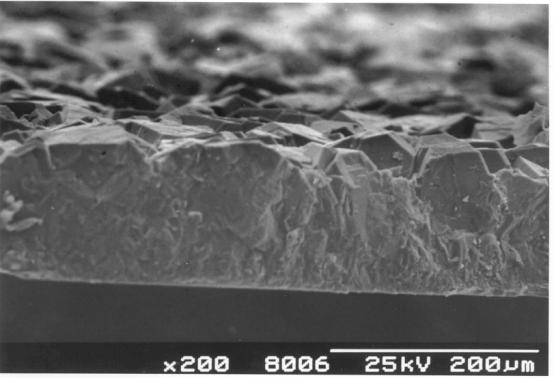
film grows. This effect could be seen in the cross-sectional SEM image of an
industrial diamond film shown in figure 2.28.
Silver dag contacts did not
give Ohmic behaviour for diamonds with low doping levels ([C]/[B] ratio below
250 p.p.m.) due to a Schottky barrier forming at the metal-semiconductor
interface. 101 Some research groups have argued that
sufficiently electronegative metals such as gold (Au) overcome this
problem 101‑103 but their work remains less than
conclusive.
2.9.3 Three Layer Metalisation
A more reliable way of
forming an Ohmic top contact was to use a “three layer metalization” technique
where three layers of metal were deposited on the surface of the diamond. The
bottom layer was a titanium (Ti) spot which could be annealed to produce a
titanium carbide (TiC) layer between the metal and the diamond. This chemical
bonding reduced the Schottky barrier at the metal-semiconductor interface and
gave the required Ohmic behaviour. A gold (Au) top layer was required to
prevent the oxidation of the titanium during the annealing step and, more
slowly, over the lifetime of the device as titanium reacts readily with any
traces of oxygen at elevated temperatures. Finally, a layer of platinum (Pt)
was required as a barrier layer between the titanium and gold layers to prevent
the interdiffusion of the metals during annealing. Wires could be attached to
the surface of the gold spot using silver dag, as before. A schematic diagram
of the design of the contacts can be found in figure 2.5. Further details of
the formation of Ohmic contacts can be found in chapter 3.
The titanium and gold layers
were deposited using a Edwards evaporator which was modified to incorporate a
heating stage. To prevent oxidation of the titanium, the substrate was heated
in vacuum to remove oxygen containing species from the surface. The titanium
evaporation was then performed on a clean surface. After the deposition, the
sample was allowed to cool down to room temperature before being exposed to
air.
The evaporator worked by
passing a current through a tungsten (W) wire basket containing the source
metal (titanium pellets or short strips of gold). A current of approximately 40
A was sufficient to evaporate the source metal. The substrate, which was
positioned under the basket, became coated by the metal as it resolidified.
Platinum possesses a high
boiling point and could only be evaporated with difficulty. Therefore, a
sputter coater was used to deposit the platinum spots.
|
Element |
Melting Point, qC,m / °C |
Boiling Point, qC,b / °C |
|
Gold (Au) |
1063 |
2970 |
|
Titanium (Ti) |
1675 |
3260 |
|
Platinum (Pt) |
1769 |
4530 |
|
Tungsten (W) |
3410 |
5930 |
Table 2.4 - Transition temperatures
of selected pure metals at standard pressure
Values taken from reference
12 and based upon IUPAC(1983) standards
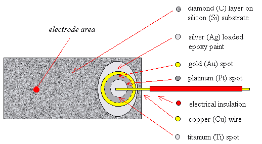
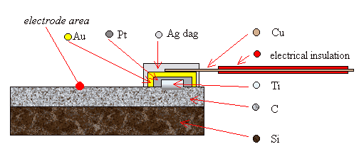
Figure 2.5 - A schematic
diagram of a three layer metal top contact (not to scale)
Note that the plan view shows the metal layers in reverse order for
illustrative purposes. The layers from top to bottom are Ag, Au, Pt & Ti
The three layer metalization
described above is the best technique used to form good Ohmic contacts to
diamond electrodes. However, the need for three separate metal depositions and
an annealing step reduce the practicality of the technique significantly. The
extensive processing may also effect the surface properties of the film.
2.9.4 Titanium Contacts
A novel method was developed
to form Ohmic contacts for the low doped diamond samples in this study. A
single strip of titanium was deposited onto the surface of the silicon
substrate before the diamond deposition. Selective diamond growth on top of
this metal layer was achieved by leaving a smooth section of silicon which
provided few nucleation sites. As the diamond formed at raised temperatures, a
metal carbide would form without the need for a separate annealing step after
the growth process and, since the film was being grown in the absence of an
oxygen containing species, no protective metals were needed to prevent
oxidation of the titanium. A schematic diagram of the design of the contacts
can be found in figure 2.6. Full details of the technique can be found in
chapter 3.
This technique greatly
simplified the processing required to fabricate a working electrode. The
platinum and gold deposition steps and the annealing process were no longer
required. The titanium deposition could be performed on the substrate before
the diamond deposition. For the three layer metalisation technique, all four of
these steps involved heating the samples above room temperature and so had the
potential to change the surface conditions of the diamond films.
The reduction of the number
of steps significantly reduced the time required to produce a working electrode
and the reliability of the overall fabrication process was dramatically
increased.
The use of a back contact
gives the maximum possible surface area for use as an electrode but requires
the film to be conductive throughout its bulk.
The presence of the titanium
strip made the use of post-treatments more complicated. Procedures such as
refluxing in nitric acid (HNO3) or dipping into chromic acid
(sat. soln. of K2Cr2O7 in conc. H2SO4)
could not be easily performed. This problem could be avoided by the use of PTFE
cells to mark out an area of the diamond film for selective post-treatment.
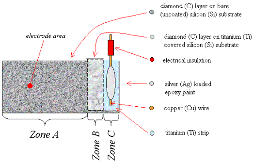
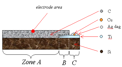
Figure 2.6
A schematic diagram of a
single layer metal bottom contact (not to scale)
Zone A is a region of diamond growth on bare silicon.
Zone B is a region of diamond growth on titanium coated silicon.
Zone C is a region of titanium coated silicon where the growth of a
continuous diamond film has been prevented by not abrading the silicon prior to
the titanium deposition.
2.9.5 Summary
The advantages and
disadvantages of the four types of contact are summarised below in table 2.5.
|
Type of Contact |
Advantages |
Disadvantages |
|
Indium/Gallium |
· does
not effect diamond film · flexibility with post- and pre-treatments · relatively convenient · no reduction in available surface area |
· need to consider diamond-silicon interface · liquid contact - less reliable · HF dip required |
|
Silver Dag |
· very convenient · does
not affect diamond film · flexibility with post- and pre-treatments |
· Schottky barriers |
|
Three Layer Metalisation |
· reliable Ohmic contacts formed |
· diamond film must be heated · time consuming · complicated - risk of failure · limits
on possible |
|
Titanium Underlayer |
· reliable Ohmic contacts formed · does
not affect diamond film · no reduction in available surface area |
· restricted post-treatments · need
to conduct through the entire depth of diamond sample |
Table 2.5 - Summary of the types of electrical contacts used
in this study
2.10 Typical Growth Conditions
Table 2.6 summarises the
typical growth conditions for the diamond films. Appendix B gives full details
of the growth conditions for the films used in these studies.
|
Pressure |
20
Torr |
|
Hydrogen
flow rate |
200
s.c.c.m. |
|
Methane
flow rate |
1.4
s.c.c.m. |
|
Diborane
flow rate (range) |
5
´ 10-6 s.c.c.m. to 5 ´ 10-2 s.c.c.m. |
|
Diborane
flow rate (typical of low end) |
4
´ 10-5 s.c.c.m. |
|
Substrate
temperature |
900
ºC |
|
Filament
temperature |
2400
ºC |
|
Filament/substrate
separation |
4
mm |
|
Deposition
Time |
7
hours to 27 hours |
|
Substrates |
Si
- see appendix B for specifications |
|
Filaments |
two
ten-turn Ti coils |
Table 2.6 - Typical
deposition conditions for the hot-filament CVD reactor
2.11 Secondary Ion Mass Spectroscopy
Secondary Ion Mass
Spectroscopy (SIMS) was used to detect the presence of boron in the films and
to determine the level of doping.
SIMS involved the
bombardment of the sample with high energy ions in an ultra-high vacuum (UHV)
chamber. On impact with the sample, the incident ions caused the ionisation of
the surface. The ions released from the surface entered an electric field which
drew them into a time-of-flight mass spectrometer (ToF‑MS). The time
taken for the ions to reach the detector was proportional to the ratio of the
mass of the ion to its electronic charge (m/z).
SIMS analysis of the diamond
films grown for this study was performed at two institutions: the University of
Bristol Interface Analysis Centre (IAC) and Millbrook Instruments Limited
(Lancashire).
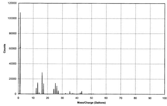
The IAC produced positive
and negative ion spectra (figures 2.7 and 2.8 respectively). The positive ion
spectrum showed peaks at m/z values of 10 and 11 daltons. This
corresponded to singly charged ions of the two isotopes of boron (10B+
& 11B+) and indicated the presence of boron in the
films. Unfortunately, without knowledge of the relative sensitivity of the
technique to the different species present, the data can not be used for
quantitative analysis of the boron concentration.
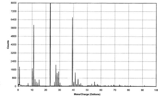
Figure
2.7 - A positive ion time-of-flight SIMS spectrum
Figure
2.8 - A negative ion time-of-flight SIMS spectrum
Four diamond samples were
sent to Millbrook Instruments for SIMS analysis. Table 2.7 shows the relevant
characteristics of the films.
Sample |
Code Number |
Concentration of boron in the gas phase [B]/[C] in p.p.m. |
Comment |
Resistance (W) |
|
(a) |
B4 |
undoped |
grown before first use of
boron containing species |
2.5 ´ 106 |
|
(b) |
B47 |
“low” |
boron contamination from
chamber |
2500 |
|
(c) |
B48 |
8.8 ´ 10-5 |
|
250 |
|
(d) |
B44 |
5.3 ´ 10-3 |
|
600 |
Table 2.7 - Samples analysed
by Millbrook Instruments using SIMS
The resistance values given
were determined using a digital voltmeter (DVM) and were intended for use only
as rough guidance.
Millbrook Instruments
provided a laboratory standard graphite sample with a known concentration of
boron (50 p.p.m.). This allowed for calibration of the spectra.
Figures 2.9 to 2.12 show the
raw spectra for the four diamond samples and figure 2.13 shows the
corresponding figure for the graphite control. The processed data are shown in
figure 2.14. The analysis conditions are summarised in table 2.8 below.
Incident
Ion |
Ga+ |
|
Beam
Intensity |
6
keV, 20 nA |
|
Raster
Area |
250
mm ´ 250 mm |
|
Mass
Range |
6
- 16 m/z (10 channels per mass) |
|
Dwell
Time |
1
second per channel |
|
Averaging |
10
scans |
|
Acquisition
Time (per spectrum) |
1000
seconds |
Table 2.8 - A Summary of the
SIMS Experimental Conditions
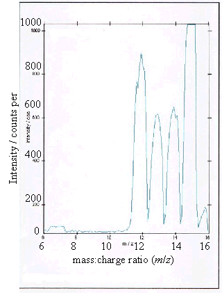
Figure 2.9 - A positive ion
time-of-flight SIMS spectrum of sample (a)
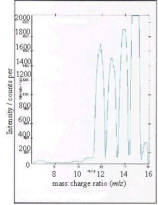
Figure 2.10 - A positive ion
time-of-flight SIMS spectrum of sample (b)
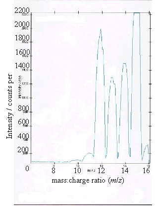
Figure 2.11 - A positive ion
time-of-flight SIMS spectrum of sample (c)
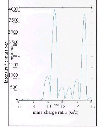
Figure 2.12 - A positive ion
time-of-flight SIMS spectrum of sample (d)
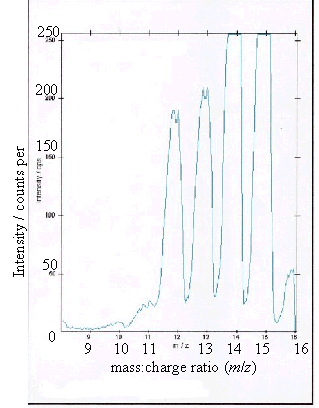
Figure 2.13 - A positive ion
time-of-flight SIMS spectrum of the graphite control
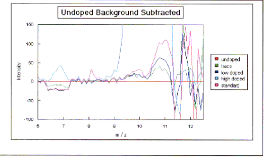
Figure 2.14 - SIMS spectra plotted relative to the undoped control
sample (a)
Adsorbed oxygen and water
enhanced the B+ signal by an order of magnitude. However, long count
times had to be employed to detect the low levels of boron and the surface was
significantly eroded. Therefore, the enhanced signal intensity at the surface
did not give a reduction of the detection limit.
As expected, samples (b),
(c) and (d) showed boron peaks at m/z values of 10 and 11. The ratio of the
intensities of the two boron peaks ranged from 80:20 to 70:30 which is in
agreement the ratio of natural abundances of the boron isotopes 10B
and 11B (81.3 : 18.7). 12
The peaks at m/z
values of 12, 13, 14 and 15 corresponded to CHx+ ions where x = 0 to 3.
Samples (a), (b) and (d) all showed a low level
contaminant peak at m/z = 7. This corresponded to lithium ions
(Li+). The intensities of the peaks indicated that the lithium
contamination was at the sub p.p.m. level.
The results suggested that the level of doping in
the films is broadly proportional to the gas phase concentrations. Previous
published work using SIMS to analyse levels of boron doping in CVD diamond had
been inconclusive. 79,104,105
As SIMS is a locally
destructive technique, it may be used to produce depth profiles where the
concentrations of the species are plotted against the depth of erosion into the
sample. Depth profiling requires long measurement times and so proved
impractical due to the hardness of diamond and its resistance to erosion.
However, in the experiments detailed here, the low levels of boron in the films
necessitated the sampling of a sufficiently large quantity of material in order
to produce reliable results that the values may be considered to apply to the
bulk rather than the surface.
It should be noted that SIMS measures the total
boron content in the films. This boron does not necessarily have to occupy
electrically active substitutional sites in the diamond crystal.
2.12 Scanning Electron Microscopy and Optical
Microscopy
Scanning electron microscopy
(SEM) and optical microscopy were the main techniques used to characterise the
films.
The SEM work was performed
on a Hitachi Model 3200 Scanning Electron Microscope operating with an
accelerating potential of 25 keV. A Mamiya camera loaded with rolls of 6 ´ 7 cm film was used to capture images.
SEM requires samples that
are electrically conductive. In order to increase the surface conductivity of
insulating samples, a layer of gold (Au) was deposited with an Edwards S150A
Sputter Coater. This treatment was not required for the boron doped diamond
samples as the doping made them sufficiently conductive.
The electron microscope was
fitted with an energy-dispersive X-ray (EDX) spectrometer designed to perform
an elemental analysis. The EDX detector was protected by a beryllium (Be)
window. This prevented the detection of X-rays from elements with low atomic
numbers such as carbon (C) and boron (B) and so the EDX spectra were of limited
use in the analysis of the boron doping of diamond.
A Zeiss Axiolab Optical
Microscope fitted with Zeiss Epiplan lenses was routinely used to view the
samples. Objective lenses of 5 ´, 10 ´, 50 ´ and 100 ´ coupled with an 10 ´ eyepiece to give a range of magnifications
from fifty to one thousand.
Images were captured with a
JVC TK-1280E Colour Camera attached to an Olympus BH2 Optical Microscope fitted
with a 10 ´ eyepiece and 4 ´, 10 ´, 20 ´ and 50 ´ objective lenses.
Optical microscopy was
particularly helpful in monitoring the deposition of titanium. Titanium layers
that had become oxidised were often blue in colour.
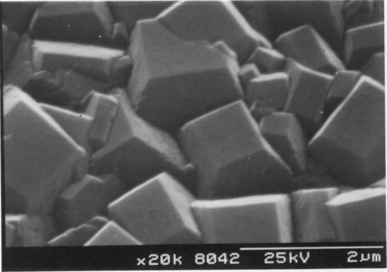
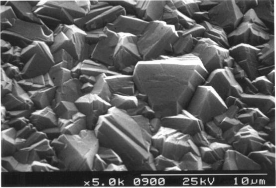
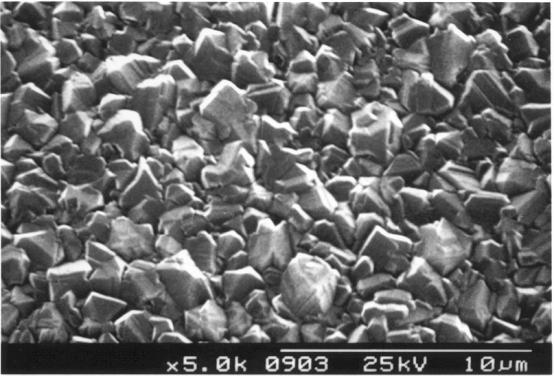
SEM and optical microscopy
showed the diamond films to be continuous and composed of well formed
crystallites. Initial experiments were performed in which the growth conditions
were varied. These confirmed that the optimum growth conditions outlined in
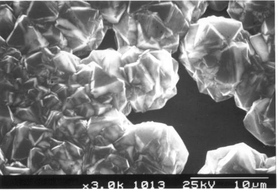
previous studies gave the best results. Figures 2.15 to 2.18 show SEM images of
an undoped diamond film grown under the typical conditions listed in table 2.6.
Figures 2.15 to 2.17 show images of the top surface at various levels of
magnification. Figure 2.18 shows a image of the cross-section of the film. The
film was uniform and has well defined, predominantly square faceted
crystallites.
Figures 2.19 and 2.20 show
diamond films grown with double and quadruple the normal concentration of
methane respectively. The films exhibited a much less well defined structure,
characteristic of growth with a high carbon to hydrogen ratio in the gas
mixture. 14,17
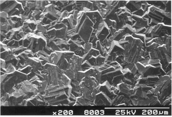
Figures 2.21 and 2.22 show
cross-sectional SEM images typical of those used to measure the thickness of
the diamond films. The rate of deposition, calculated by dividing the thickness
of the diamond by the growth time, varied between films from zero to 0.7 mm/hr.
Within each growth run, the
rate of deposition was expected to vary. Initial nucleation had to occur before
a continuous film could start to form. Growth would then progress on different
crystal faces at different rates. The gradual reaction of the hot filaments or
any other changes in the reaction conditions may have added to any variations
in the rate of growth.
The thickness of thirty
samples, which had grown beyond the nucleation phase and formed continuous
films, was measured. The mean growth rate was 0.3 ± 0.2 mm/hr. No significant
difference in the rate of deposition was detected between boron doped and
undoped diamond films.
Figure
2.15 - The surface of a HFCVD diamond film showing
square
facets and a twinned crystallite [sample B13]

Figure 2.16
- The surface of a HFCVD diamond film [sample B13]
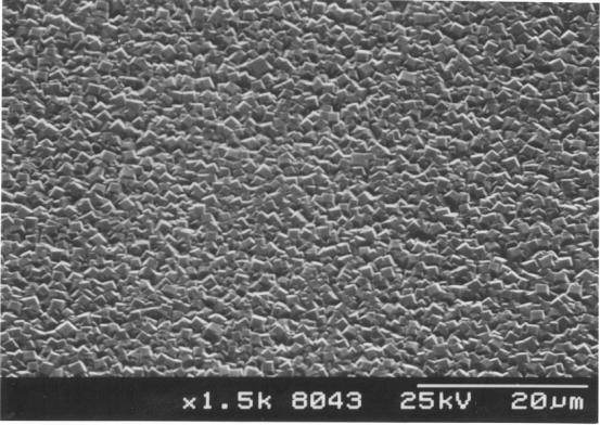
Figure 2.17 - The surface of a HFCVD
diamond film
showing
uniform coverage over the substrate [sample B13]
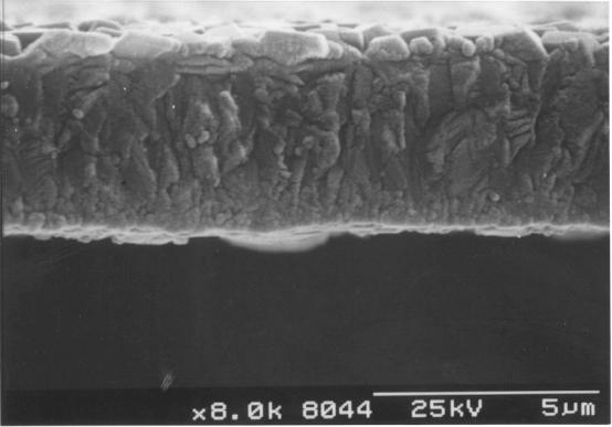
Figure
2.18 - A cross-section of a diamond film [sample B13]
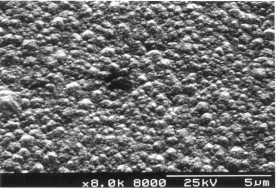
Figure 2.19 - A
diamond film grown in an atmosphere containing 1.4% methane
(double
the normal concentration) [sample B6]
Figure 2.20 - A
diamond film grown in an atmosphere containing 2.8% methane
(quadruple
the normal concentration) [sample B8]
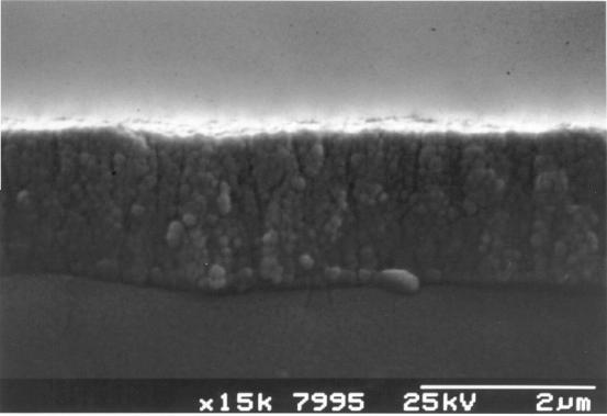
Figure 2.21 - A
cross-sectional view of a diamond film grown with quadruple
the normal
concentration of methane in the gas phase [sample B8]
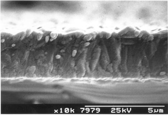
Figure 2.22 - A
cross-sectional view of the results of an early growth run
[sample
B1]
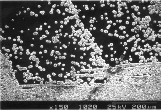
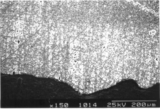
Figures 2.23 to 2.25 show
images of a sample where the diamond growth had been stopped after 5 hours and
35 minutes. Figure 2.23 shows the surface at the centre of the sample where the
diamond film was continuous with well defined facets. Figures 2.24 and 2.25
show the surface at the periphery of the sample where the growth has not
progressed far beyond the nucleation stage, leaving individual crystallites on
the silicon substrate.
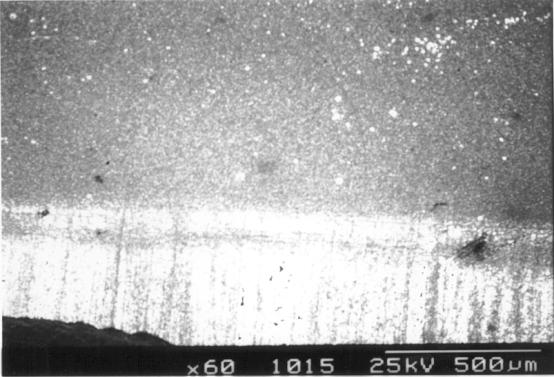
The quality and morphology
of the films was comparable to that obtained in industrially grown samples.
Figures 2.26 to 2.28 show an industrial free-standing diamond film that was
grown for an optical application in the aerospace industry using microwave
plasma assisted CVD (MPACVD). 106 The industrial film was grown
continuously for about ten days 107 and is therefore much thicker
(175 mm) than the HFCVD films and it exhibits
larger facet sizes (~50 mm).
Figures 2.29 and 2.31 show
various views of a thin diamond film.
Figure
2.23 - A continuous diamond film [sample B142a]
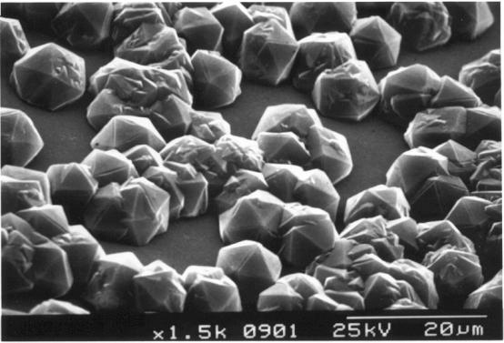
Figure 2.24 -
Incomplete surface coverage at the edge of a thin diamond film.
The silicon substrate
was visible behind the diamond crystallites [sample B142a]
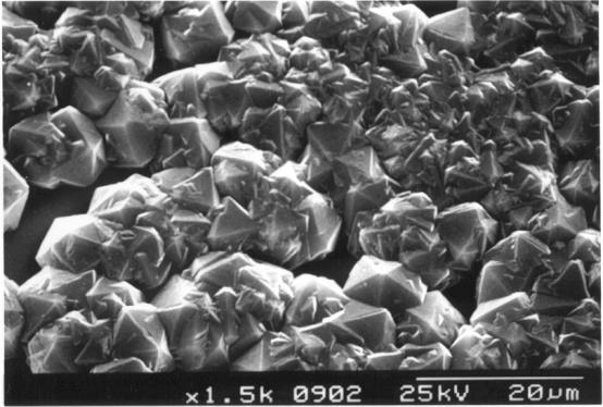
Figure 2.25 - The
reaction stopped at the stage where the individual crystallites
have
started to coalesce to form a continuous film [sample B142a]
Figure
2.26 - Industrial MPACVD diamond (undoped)
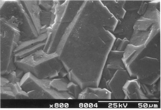
Figure
2.27 - Industrial MPACVD diamond (undoped)
Figure
2.28 - A cross-section of a free-standing industrial
MPACVD
diamond film
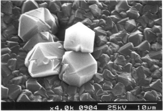
Figure 2.29 - SEM
image showing large crystallites formed around 2-3 mm
diamond
crystals remaining from the substrate abrasion process [sample B141b]
Figure
2.30 - SEM image showing growth of a thin diamond film
[sample
B141b]
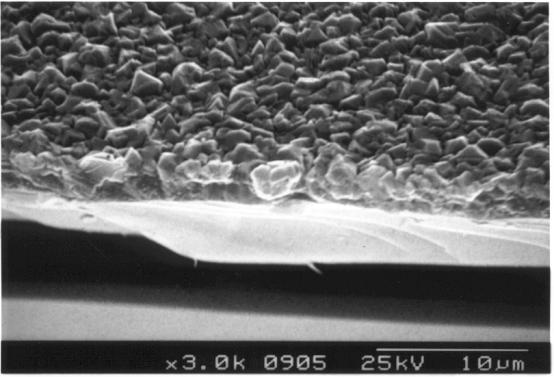
Figure 2.31 -
SEM image showing a cross-section of a thin diamond film
[sample
B141b]
The titanium contacts
described in section 2.9.4 required three distinct zones of diamond growth.
·
The
main section of the sample had to comprise of a continuous film of high quality
diamond grown directly over an insulating silicon substrate. This zone would
form the electrode surface in the electrochemical experiments.
·
An
exposed titanium strip was required at the edge of the sample to allow
electrical connections to be made.
·
Finally,
a middle zone is required comprising of diamond grown over titanium. This zone
would form the Ohmic contact between the metal and the semi‑conducting
diamond.
The standard electrode
design had a single strip of titanium (as shown in figure 2.6). This was
ideal for the electrochemical studies as the design maximised the surface area
of usable diamond. The single strip design did not, however, readily facilitate
studies of the contact itself. The absence of a second Ohmic contact
complicated measurements of the current-voltage characteristics. To avoid this
problem, a diamond sample was made with two titanium strips, on opposing edges
of the sample, as shown in figure 2.32. The electrical properties of this film
were investigated as detailed in chapter 3.
Figures 2.33 to 2.60 show
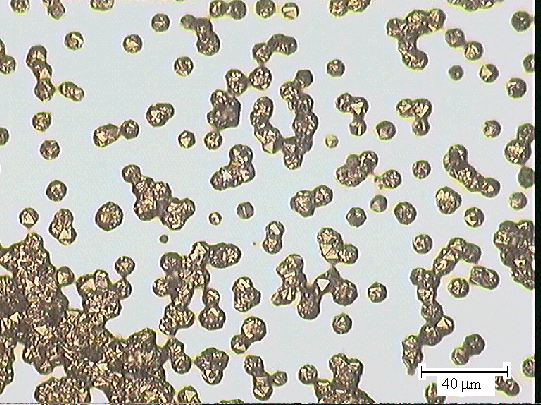
SEM and optical images of the double ended sample (B147a). The sample has good
coverage where required (zones 2 to 4) and incomplete coverage where the
titanium needs to be exposed (zones 1 and 5). The two end zones were prepared
in the same way: a coating of titanium was applied to a clean, smooth, unabraded
silicon surface. However, the extent of diamond growth on these zones varied
considerably. Zone 5 was typical of growth on unabraded substrates: isolated
crystallites formed with minimal overall coverage. Zone 1 was unusual in that
there was much greater coverage than normal. The growth had progressed beyond
the nucleation stage and the crystallites had started to coalesce. The
increased coverage did not, however, provide complete coverage and good
electrical contacts could still be made to the exposed underlying titanium.
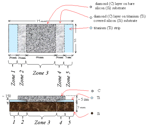
Figure 2.32 - A schematic
diagram of sample B147a (not to scale)
Zone 3 is a region of diamond growth on bare silicon.
Zones 2 & 4 are regions of diamond growth on titanium coated
silicon.
Zones 1 & 5 are a regions of titanium coated silicon where the
growth of a continuous diamond film has been prevented by not abrading the
silicon prior to the titanium deposition.
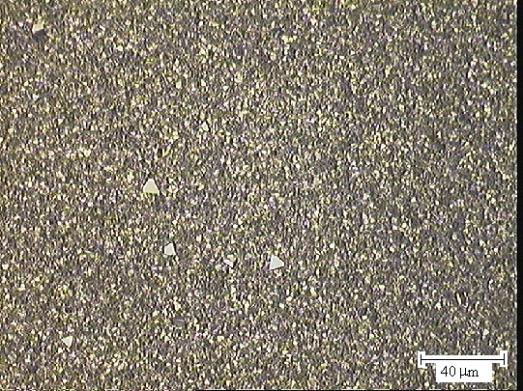
Figures 2.33 to 2.36 show
four optical microscopy images of the central section of the surface (zone 3)
taken with a 50 ´ objective lens. The images
were taken at well spaced points across zone one and show the uniformity of the
film. Figure 2.37 shows a smaller scale image taken with a 20 ´ objective lens. SEM images of zone 3 are
shown in figures 2.38 and 2.39.
As described in section 2.8,
2-3 mm
diamond grit was used in the preparation of the substrates. The majority of the
diamond grit was removed from the silicon surface before the substrate was
loaded into the CVD chamber. Any remaining diamond crystals that survived the
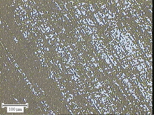
cleaning process acted as nucleation sites for diamond growth. Figure 2.28
shows a SEM image of diamond crystallites formed from such growth. Optical
microscopy clearly showed these crystallites as any facets orientated normal to
the incident light beam would shine brightly as they reflected the light back
towards the optical system. A number of isolated square and triangular facets
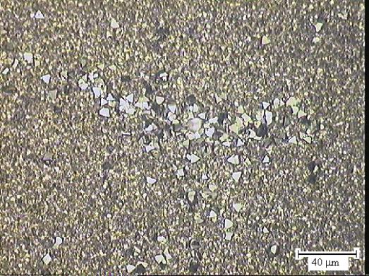
can be seen in figures 2.33 to 2.35, while 2.36 shows a conglomeration of them.
Figures 2.34 and 2.37 show complete crystallites, highlighted by red circles,
in which none of the facets are perpendicular to the normal illumination.
Sample B147a contained
larger numbers of these crystallites than were normally seen in the diamond
films. The presence of two titanium strips on the substrate made the abrasion
and cleaning process more complicated. It was necessary when cleaning the
surfaces of the abraded regions (zones 2 to 4) to keep the surfaces of the end
regions (zones 1 & 5) free from diamond grit and so, in order to prevent
contamination, a less rigorous cleaning procedure was performed.
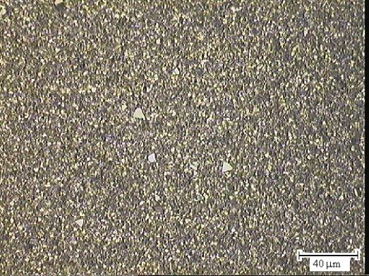
Figures 2.33 & 2.34 - optical microscopy images of the central
section (zone 3),
50 ´ objective lens, red circle
highlights a crystal (see page 67) [sample B147a]
Figures 2.35 & 2.36 - optical microscopy images of the central
section (zone 3)
taken with a 50 ´ objective lens [sample
B147a]
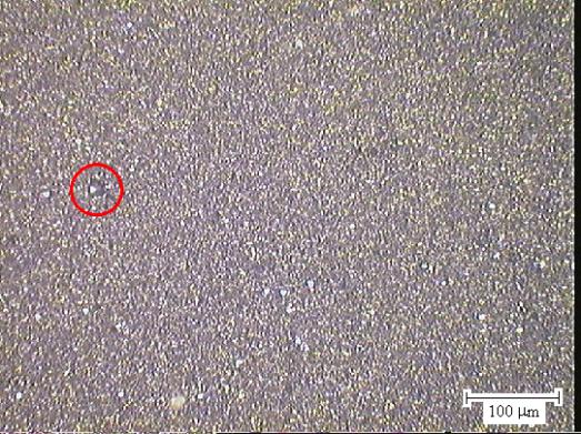
Figure 2.37 - optical microscopy image of the central section (zone 3),
20 ´ objective lens, red circle highlights a
crystal (see page 67) [sample B147a]
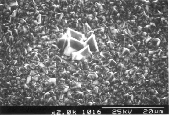
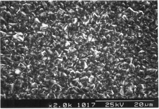
Figure 2.39 - SEM image of the central section (zone 3) [sample B147a]
As expected, the growth of diamond
on zones 1 and 5 did not totally cover the underlying titanium.
Zone 5 was typical of the
films grown on smooth titanium covered silicon, in that there was only isolated
diamond growth. Figure 2.40 shows an optical image of the sample taken with a
50 ´ objective lens. The lower left hand side
showed some coalescing of the individual cystallites but the majority of the
area was covered only by well spaced, isolated crystallites. Figure 2.41 shows
a similar image, in which a continuous narrow strip of diamond could be seen,
probably formed along a microscopic scratch on the surface of the silicon.
Figure 2.42 shows an area of
denser coverage nearer the adjacent abraded region (zone 4) and figure 2.43
shows an optical image taken at a lower resolution (20 ´ objective lens). Figure 2.44 and 2.45
show SEM images of zone 1 of the film. The detail of an individual crystallite
can be seen in figure 2.45.
The opposite end of the
sample (zone 1) exhibited unusually good diamond coverage, comparable to the most
extensive growth seen on any of the unabraded titanium strips in this study.
Figures 2.46 and 2.47 show optical images of zone 1 taken with a 50 ´ objective lens and figures 2.48 and 2.49
show the region viewed with a 20 ´ objective lens. Figure 2.50
shows an SEM image of zone 1. The images show that although there was
considerable diamond coverage, there were still areas of exposed titanium. Good
electrical contact could therefore be made to this region.
Figures 2.40 & 2.41 - optical microscopy images of one of the end
sections
(zone 5) taken with a 50 ´ objective lens
showing limited diamond growth [sample B147a]
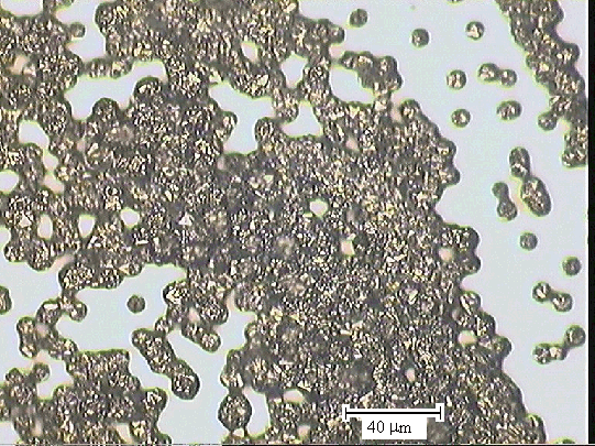
Figure 2.42 - optical microscopy image of taken with a 50 ´ objective lens
showing partial diamond growth [sample B147a]
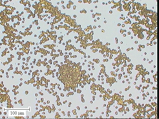
Figure 2.43 - optical microscopy image of one of the end sections (zone
5)
taken with a 20 ´ objective lens [sample
B147a]

Figure 2.44 - SEM image of one of the end sections (zone 5) [sample
B147a]
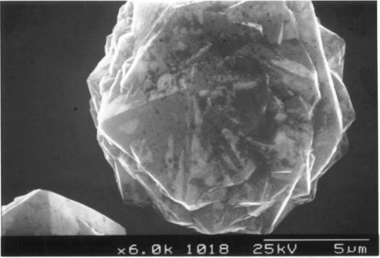
Figure 2.45 - SEM image of one of the isolated diamond crystallites
[sample B147a]
Figures 2.46 & 2.47 - optical microscopy images of one of the end
sections
(zone 1) taken with a 50 ´ objective lens showing
partial diamond growth
[sample B147a]
Figures 2.48 & 2.49 - optical microscopy images of one of the end
sections
(zone 1) taken with a 20 ´ objective lens showing
partial diamond growth
[sample B147a]
Figure
2.50 - SEM image of one of the end sections (zone 1)
showing
partial diamond growth [sample B147a]
The boundaries between the
growth zones can be seen in figures 2.51 to 2.57 (optical microscopy) and
figures 2.58 to 2.60 (SEM).
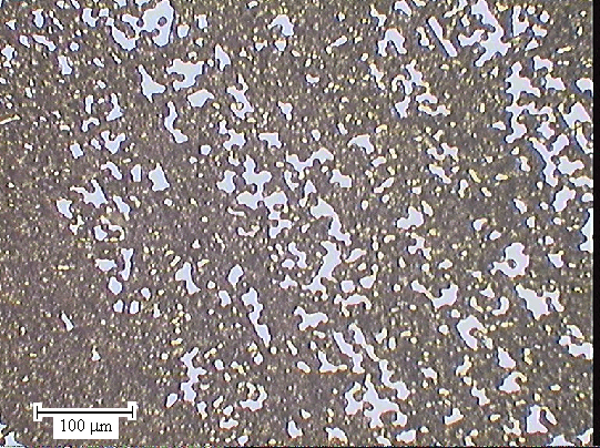
Figures 2.51, 2.52 and 2.58
show the clearly defined boundary between zones 4 and 5.
Figures 2.51 and 2.58 show
the same region viewed by optical and electron microscopy respectively.
Measurement of the distances between distinctive features visible in both the
images allowed an accurate scale to be applied to the optical images presented in
this chapter.
Figures 2.53 and 2.54 show
the boundary at the opposite end of the sample (between zones 1 and 2). There
was less difference between the diamond coverage in these two zones but the
boundary could still be identified.
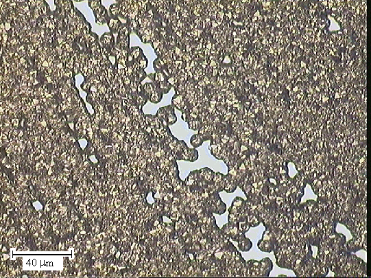
Figure 2.55 shows the
boundary between zones 3 and 4. There is complete diamond coverage over both
regions. The transparency of the diamond film allowed light to pass through the
sample. Zone 4 appeared brighter than zone 3 as the titanium beneath zone 4
reflected more light than the silicon beneath zone 3.
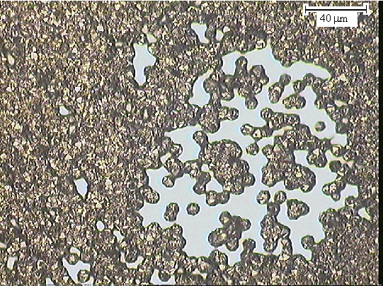
Figures 2.56 and 2.57 show
the boundary between zones 2 and 3. As for the boundary between zones 3 and 4,
the diamond coverage was complete and reflection from the underlying titanium
could be seen.
Figures 2.59 and 2.60 show
SEM images of the boundary between zones 1 and 2. Zone 2 can be seen at the top
of the images with zone 5 beneath it. The dark areas at the bottom of the
images showed the silver dag which had been used to make electrical contacts to
zone 1.
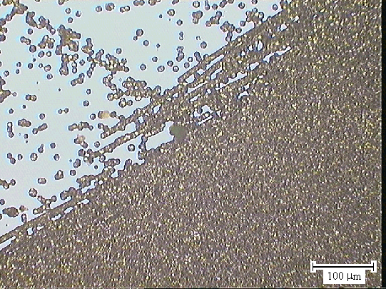
Figure 2.51 - the boundary between zones 4 and 5 (´ 20 lens) [sample B147a]
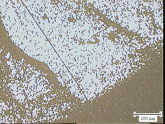
Figure 2.52 - the boundary between zones 4 and 5 (´ 10 lens) [sample B147a]
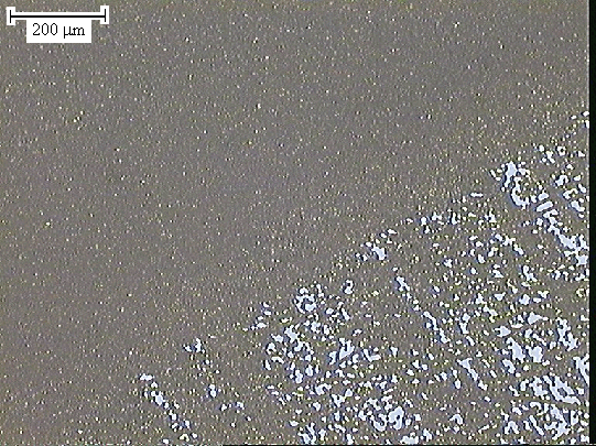
Figure 2.53 - the boundary between zones 1 and 2 (´ 10 lens) [sample B147a]
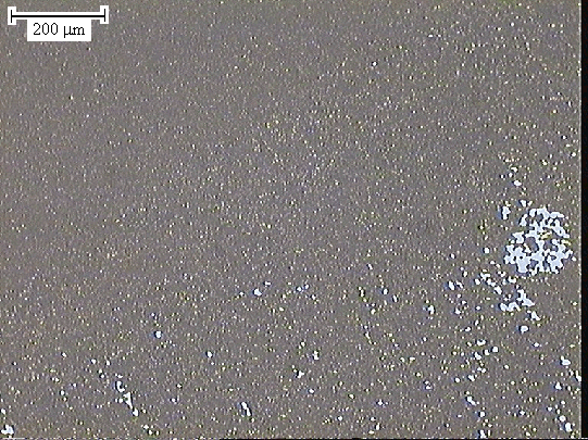
Figure 2.54 - the boundary between zones 1 and 2 (´ 10 lens) [sample B147a]
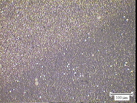
Figure 2.55 - the boundary between zones 3 and 4 (´ 20 lens) [sample B147a]
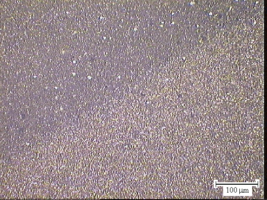
Figure 2.56 - the boundary between zones 2 and 3 (´ 20 lens) [sample B147a]
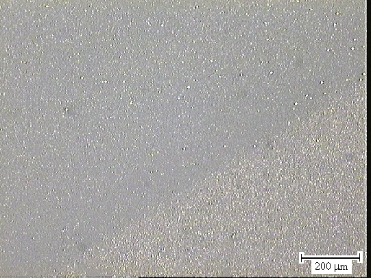
Figure 2.57 - the boundary between zones 2 and 3 (´ 10 lens) [sample B147a]
Figure
2.58 - SEM image of the boundary between zones 4 and 5
[sample
B147a]
Figure
2.59 - SEM image of the boundary between zones 1 and 2
[sample
B147a]
Figure
2.60 - SEM image of the boundary between zones 1 and 2
[sample
B147a]
2.13 Laser Raman Spectroscopy
Raman Spectroscopy is a well
established diagnostic technique for determining the quality of diamond films. 108-112
Spectra of diamond show a characteristic peak at a shift of 1332 cm-1
relative to the excitation wavenumber. The peak is the highest energy Raman
peak for diamond and corresponds to the zero phonon excitation in the crystal.
In good quality diamond samples, this peak is sharp. However, if the crystal
structure is distorted then the spread of the peak, as measured by the
full-width half-maximum, will increase and the peak may be shifted up or down
the spectrum.
As well as the diamond peak
at 1332 cm-1, a number of other Raman peaks may be seen in poor
quality diamond films. Graphite produces peaks at 1580 cm-1 and
1355 cm-1 and disordered sp2 carbon produces an
asymmetrical broad band from 1100 cm-1 to 1600 cm-1 with
a maximum at around 1520 cm-1.
Raman spectroscopy can be a
very sensitive technique in detecting small amounts of graphitic content in
diamond films. When the incident laser beam with an excitation wavelength of
488 nm is chosen, the technique is fifty times more sensitive to sp2
structures than to sp3 structures.
In addition to Raman peaks,
the laser illumination can also lead to photoluminescence (PL) peaks due to
impurities and structural defects.
Raman spectroscopy provides
an excellent tool to gain qualitative information on the quality of diamond
films.
Several studies have reported
changes to the Raman spectrum due to the presence of boron in the diamond
films. These changes require higher levels of doping than can be those present
in the films presented here
(50 p.p.m., 9 ´ 1018 B atoms/cm3).
Raman spectra were taken with
a Renishaw Raman Imaging Microscope and Spectrometer with a spectral resolution
of 1 cm-1. An argon gas laser with a wavelength of 488 nm (green
light) was used to provide the incident laser beam.
Figure 2.61 shows a Raman
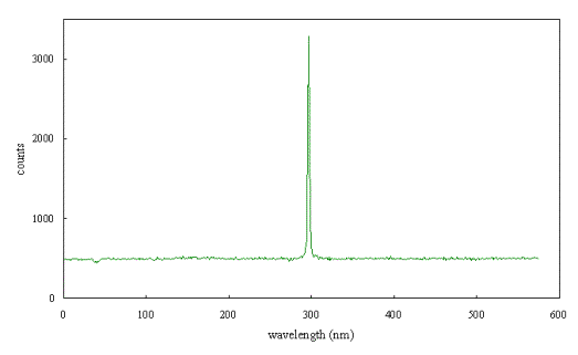
spectrum of a natural type IIb diamond crystal.*
A single sharp peak can be seen which was used to calibrate the spectrometer.
Figure 2.62 shows a Raman
spectrum of an poor quality undoped diamond film grown by MPACVD which provides
an example of some of the features that may be seen in diamond films. The 1332
cm-1 diamond peak is visible but is not particularly sharp and not
larger than the other features. A broad peak centred around 1355 cm-1
due to graphite and disordered sp2 carbon and a broad band centred
at around 1500 cm-1 can be seen. The broad band shows some fine
structure that may be due to impurities or defects (such as nitrogen centres).
The fine structure can not be readily assigned from a spectrum taken at room
temperature.
Figures 2.63 to 2.68 show
Raman spectra of diamond films grown for this study. While there was some
variation in the spectra, they all displayed a sharp 1332 cm-1
diamond peak. There was some evidence of a broad band due to disordered sp2
carbon but this was weak and therefore confirmed that there was little sp2
carbon present in the films.
zero‑phonon
peak and no other significant features
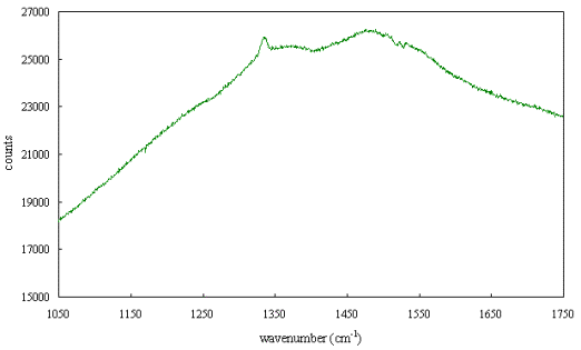
Figure 2.62 - Raman spectrum of a poor quality undoped MPACVD
diamond
film
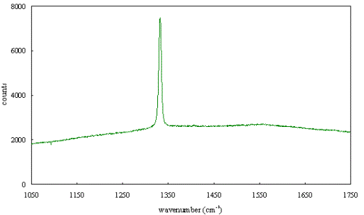
Figure 2.63 - Raman spectrum of boron doped diamond [sample B128a]
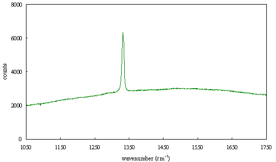
Figure 2.64 - Raman spectrum of boron doped diamond [sample B128b]
Figure 2.65 -
Raman spectrum of boron doped diamond [sample B129a]
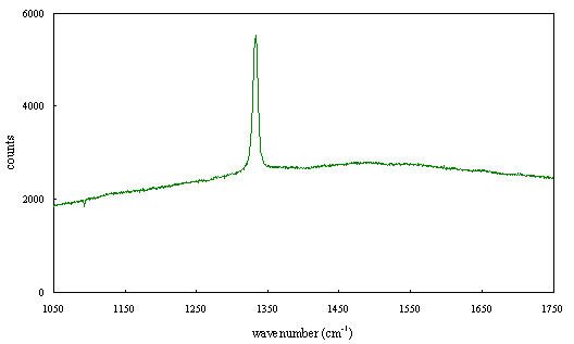
Figure 2.66 - Raman spectrum of boron doped diamond [sample B130b]
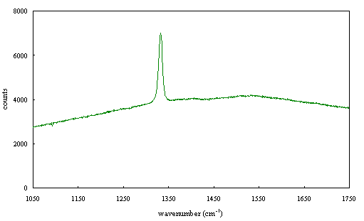
Figure 2.67 - Raman spectrum of boron doped diamond [sample B140a]
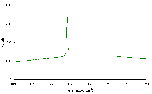
Figure 2.68 - Raman spectrum of boron doped diamond [sample B140b]
2.14 Summary
CVD apparatus has been
assembled which can deposit boron doped polycrystalline diamond films with a
wide range of doping levels.
SIMS, SEM and optical
microscopy have been used to show the films to be continuous and of high
quality.
Diamond films have been
deposited selectively onto patterned silicon wafers. The use of patterned
silicon wafers with a partial titanium covering provided a novel method to
fabricate boron doped diamond films with good Ohmic contacts.
† Chromic acid was prepared immediately before use by making a saturated a saturated solution of potassium dichromate (K2Cr2O7) in concentrated sulphuric acid (H2SO4). 134
† The manufacturer of the diborane gas used in these studies required approximately six months to produce and deliver a standard order of diborane. Supplies of more esoteric gases, such as the trimethylboron (B(CH3)3) used in references 76 and 77 were not as readily available.
‡ Vaporisation has been used as an alternative to dissolution for solid B2O3 sources 92 but problems with controllability remain.
* Type II is a classification established in 1934 for diamonds transparent to 8 mm infra-red radiation. It was subsequently discovered that the diamonds that are opaque to 8 mm radiation, and hence classified as type I, contain nitrogen impurities. 5 Type IIb signifies a very low concentration of nitrogen.
![]()