Chapter 2
Diamond Growth
and Characterisation
2.1.
Background
2.1.1. Introduction
Diamond is one of the hardest natural materials, has one of the highest thermal conductivities at room temperature, is transparent over a very wide wavelength range, is one of the stiffest materials, one of the least compressible, and is inert to most chemical reagents at room temperature. With these remarkable properties, diamond has sometimes been referred to as “the best natural material.”
Unfortunately, it has proved
very difficult to exploit these properties, due to the cost, the lack of
abundance of large natural diamonds and the fact that diamond until recently
was only available in the form of stones or powder. It had been known for 200 years
that diamond is composed only of carbon 1.
Many efforts have been made to synthesize diamond artificially
using as a starting material another commonly occurring form of carbon,
graphite (see figure 1.1). This has proved very difficult, mainly because at
room temperature and pressure, graphite is the thermodynamically stable
allotrope of carbon. Although the standard enthalpies of diamond and graphite
only differ by 2.9 kJ mol-1 2, a large activation barrier separates the two phases
avoiding interconversion between them at room temperature and pressure. This
large energy barrier is also responsible for its existence. When diamond is
formed, it does not spontaneously convert to the graphite phase. For this reason,
diamond is said to be metastable, that is kinetically stable but not
thermodynamically stable.
2.1.2. High-pressure high-temperature technique
Knowledge of the conditions
under which natural diamond is formed suggests that diamond can be formed by
heating carbon under very high pressure. This process forms the basis of the
high-pressure high-temperature (HPHT) growth technique 3. In this process graphite is compressed in a
hydraulic press to tens of thousands of atmospheres, heated to over 2000 K in
the presence of a suitable metal catalyst, and left until diamond crystallises.
The diamond crystals thus
produced are used for a wide range of industrial processes, which use the
hardness and wear resistance properties of diamond, such as cutting and
machining components and the polishing and grinding of optics. However, the
disadvantage of the HPHT method is that it still produces diamond in the form
of single crystals ranging in size from nanometers to millimetres, limiting the
range of the applications for which it can be used.
2.1.3. Chemical vapour deposition technique
The production of diamond
via the addition of carbon atoms one-at-a-time to an initial template, was fist
postulated in 1955 4. It was suggested that if this could be accomplished,
the much lower gas pressures that HPHT, there would be an advantage in terms of
equipment and energy cost.
These ideas promoted the experiments of Eversole 5 and Deryagin et
al. 6, in which thermal decomposition of carbon-containing
gases under reduced pressure was used to grow diamond on the surface of natural
diamond crystals heated to 900 oC. However, the rate of growth in
these early experiments was low, since graphite was co-deposited with the
diamond leading to impure mixed phases. Diamond synthesis advanced in the late
1960s, when Angus’s group discovered that the presence of atomic hydrogen
during the deposition process would lead to preferential etching of the
graphite, rather than diamond 7,
8.
Subsequent Russian work
showed that such chemical vapour deposition (CVD) techniques could be used to
grow diamond on non-diamond substrates 9,
10.
In 1982 Japanese researchers
at the National Institute for Research in Inorganic Materials (NIRIM) brought
all these findings together to build a “hot filament reactor”, which grew good
quality diamond films on non-diamond substrates at significant rates (ca. 1mm h-1)11, 12. The following year the same group reported another
method for achieving diamond growth, using a microwave plasma reactor 13, 14.
2.1.4. Hot Filament CVD
Hot Filament CVD (HFCVD)
involves a gas phase chemical reaction occurring above a solid surface, which
causes deposition onto that surface; the gas phase reaction activation requires
a source of energy, in this case, a hot filament.
Normal conditions in this
type of CVD chamber employ a precursor gas (usually CH4) which is
diluted in an excess of hydrogen in a typical mixing ratio of 1% by volume. The
vacuum chamber is continually pumped using a rotary pump, while process gases
are measured at carefully controlled rates (typically a total flow rate of a
few hundred s.c.c.m.). Throttle
valves keep the pressure in the chamber at typically 18-35 Torr, while a
substrate heater is used to bring the substrate up to a temperature of 750-950oC.
The substrate to be coated e.g. a piece of silicon or molybdenum is placed on
the heater, a few millimetres underneath the filament, which is electrically
heated to temperatures of about 2300oC. The filament is made from a
metal that will be able to survive these conditions and not react significantly
with the process gases. Metals like tungsten and tantalum are frequently used,
although they slowly react with the carbon-containing gases to form the metal
carbide. This changes their resistivity and makes them brittle, reducing their
lifetime and hence limiting the maximum deposition time of a single run.
This HFCVD method is
relatively cheap and easy to operate. It produces polycrystalline diamond films at a rate about 1-12 mm h-1, depending on the deposition
conditions. However, it has some disadvantages. The hot filament is
particularly sensitive to oxidizing or corrosive gases. This limits the
different gas mixtures which could be employed. It is also very difficult to
avoid contamination of the diamond film with filament material. For diamond to
be used in mechanical applications, metallic impurities at the tens of ppm
level are not a very significant problem. Diamond materials with this level of
metal contamination are not acceptable for electronic applications.
2.1.5. The choice of substrates for growing CVD diamond
The choice of substrates
depends on several criteria, some of them very simple. One of the requirements
is that the melting point (at the process pressure) must be higher than the
temperature required for diamond growth (normally greater than 750ºC). Next is
that the substrate material should have a thermal expansion coefficient
comparable with that of diamond. At the high growth temperatures currently
used, a substrate will expand. Therefore the diamond coating will be grown upon
and bonded directly to an expanded substrate. During the cooling stage, the
substrate will contract back to its room temperature size. The diamond coating
(with its very small expansion coefficient) will be relatively unmodified by
the temperature change. Hence the diamond film will experience significant
compressive stresses from the shrinking substrate, leading to bending of the
sample, and/or cracking or even delamination of the whole film.
In order to form adherent
films, it is necessary that the substrate material be able to form a carbide
layer. The reason is because diamond CVD on non-diamond substrates usually
requires the formation of a thin carbide interfacial layers, on which the
diamond then grows. The carbide has been described as the “glue” 15 which promotes growth of diamond and helps its adhesion
by (partial) relief of the stresses at the interface (caused by lattice
mismatch or substrate contraction).
Focusing on carbon substrate
interactions, any substrate material can be divided into three categories,
based upon their reactivity with carbon:
·
Little or no solubility or
reaction with carbon.
These materials
do not form a carbide layer. Therefore a diamond layer will not adhere well to the surface. This can be
used as a method to make free-standing diamond films, as the films will
frequently delaminate after deposition. This category includes metals like
copper, tin, lead, silver and gold, as well as non-metals like germanium,
sapphire and alumina.
·
Substantial mutual
solubility or reaction with carbon.
The substrate acts as a carbon sink, and deposited carbon dissolves into the surface, forming a solid solution. This can result in large quantities of carbon being transported into the bulk, rather than remaining at the surface (where it can promote diamond nucleation). Frequently diamond growth only begins after the substrate is saturated with carbon, and this can dramatically modify the physical properties of the resulting composite. Metals where this is significant include platinum, palladium, rhodium, nickel, titanium and iron (iron and stainless steel cannot be coated using simple CVD methods)
·
Carbide formation.
These include
metals like titanium, zirconium, vanadium, hafnium, tantalum, chromium,
molybdenum, cobalt, tungsten, nickel, iron, yttrium, aluminium, and certain
other rare-earth metals. In some metals such as titanium, the carbide layer
continues to grow during diamond deposition and can be hundreds of micrometers
thick. Such thick interfacial carbide layers may dramatically affect the
mechanical properties and therefore the utility of the diamond coatings on
these materials. A non-metal, such as boron or silicon, and silicon-containing
compounds such as silica (SiO2), quartz and Si3N4,
also form carbide layers. Substrates composed of carbides themselves, such as
silicon carbide (SiC), tungsten carbide (WC) and titanium carbide (TiC) are
often used for diamond deposition.
The difficulties associated
with diamond growth on problematic materials have ensured the continuing
popularity of silicon as a substrate material. It has a sufficiently high
melting point (1956ºC), it forms only a localised carbide layer (a few
nanometres thick), and it has a relatively low thermal expansion coefficient.
Molybdenum and tungsten display similar properties. These two metals are also
widely used as substrate materials.
2.1.6. Nucleation
Growth of diamond begins
when individual carbon atoms nucleate onto the surface to initiate the
beginnings of an sp3 tetrahedral lattice.
There are two different
types of diamond growth:
·
Homoepitaxial growth.
Using natural
diamond substrates, the template for the required tetrahedral structure is
already there, and the diamond lattice is just extended atom-by atom as
deposition proceeds.
·
Heterojunction growth.
Using
non-diamond substrates, there is no such template for the C atoms to follow,
and those C atoms that deposit in non-diamond forms are immediately etched back
into the gas phase by reaction with atomic H.
To deal with the
problem of the initial induction period before which diamond starts to grow,
the substrate surface often undergoes a pre-treatment prior to deposition in
order to reduce the induction time for nucleation and to increase the density
of the nucleation sites. There are two main methods to apply this
pre-treatment:
(a) Manual abrading. Abrasion of the substrate surface using diamond powder ranging in size from 10nm to 10 mm. It is believed that such polishing helps nucleation by either:
·
creating
appropriately shaped scratches in the surface, which act as growth templates,
·
embedding
nanometre-sized fragments of diamond into the surface, which then act as seed
crystals,
·
a
combination of both.
(b) Ultrasonic agitation. A better-controlled version of abrasion of
the surface is to use ultrasonic agitation to abrade the substrate immersed in
a solution of diamond powder in water or 2-propanol (IPA).
2.1.7. The CVD diamond film
When individual diamond
crystallites have nucleated on the surface, growth continues in three
dimensions until the crystals coalesce. At this point a continuous film is
formed and the only way growth can proceed is upwards. The resulting film is
polycrystalline with many grain boundaries and defects, and exhibits a columnar
structure extending upward from the substrate. Furthermore, as the film becomes
thicker, the crystal size increases while the number of defects and grain
boundaries decreases. This means that the outer layers of thicker films are
frequently much better quality than the initial nucleating layers.
The surface morphology of the
diamond film obtained during CVD depends dramatically on several process
conditions, especially the gas mixing ratio. In CH4/H2
systems, depending upon the ratio of methane to hydrogen, the film can be
randomly oriented (see figure 2.1) or have some degree of preferred
orientation, such as (111) triangular or (100) square facets. With increasing
methane concentrations, the crystal sizes decrease, until above ca. 3% CH4
in H2 the crystalline morphology disappears altogether (see figure
2.2). Such film is referred to as “nanocrystalline” or “ballas” diamond, and
may be considered to be an aggregate of diamond nanocrystals and disordered
graphite. Although this type of film might be considered inferior to the more
crystalline and therefore better quality diamond films, it still possesses many
of the desirable properties of diamond while being much smoother and
considerably faster to deposit. Thus, by the simple tactic of changing the
growth conditions, diamond films can be deposited with properties ranging from
almost graphite to essentially those of natural diamond. This allows the
quality, appearance and properties of a diamond film, as well as its growth
rate and cost, to be easily designed to suit particular applications.

Figure 2.1. Randomly oriented surface of a HFCVD (sample B13)
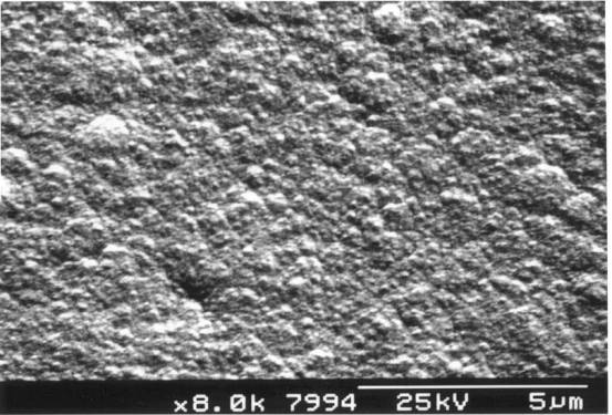
Figure 2.2. HFCVD Diamond film grown in an atmosphere
containing 2.8 % methane (“ballas” diamond) (sample B8)
2.1.8. The chemistry of CVD diamond growth
The complex chemical and
physical processes which occur during diamond CVD compromise several different
but interrelated features, and are illustrated in the figure 2.3. The process
gasses first mix in the chamber before diffusion toward the substrate surface.
They pass through an activation region, e.g. a hot filament, which provides
energy to the gaseosus species. This activation causes molecules to fragment
into reactive radicals and atoms, creates ions and electrons, and heats the gas
up to temperatures reaching a few thousand kelvins. Beyond the activation
region, these reactive fragments continue to mix and complete a complex set of
chemical reactions until they strike the substrate surface. At this point the
species either adsorb and react with the surface, desorb again back into the
gas phase, or diffuse around close to the surface until an appropriate reaction
site is found. If surface reaction occurs, one possible process, if all the
conditions are suitable, is the growth of diamond.
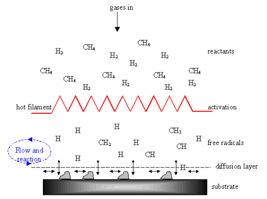
Figure 2.3. Schematic diagram of the physical and chemical processes during diamond CVD.
There have been many studies
of the gas phase chemistry 16 in the last 10 years aimed at obtaining a clear
picture of the principles involved. The first clue was obtained from the
“Bachmann triangle diagram” 17, which is a C-H-O composition diagram based upon over
70 deposition experiments in different reactors and using different process
gases. Bachmann found that independent of the deposition system or gas mixture,
diamond would only grow when the gas composition was close to and just above
the CO tie-line (see figure 2.4). This means that diamond growth was
independent of the nature of the gas phase precursors, and that the gas phase
chemistry was so rapid it simply and effectively broke down the constituent
gases to smaller, reactive components.
There have been many
suggestions for the species involved in diamond growth; including C, CH, C2, C2H,
CH3, C2H2, CH3-, and
diamondoids, such as adamantine. However, since diamond can be grown in systems
which have few ions present (e.g. HFCVD reactors), this suggests the growth
species must be neutral moieties. Further numerical simulations have shown that
diamond growth can be accounted for by a single growth species and a single
surface mechanism. A number of studies have been performed to try to identify
the growth species chemistry 16, and the general consensus is that CH3 is
the important radical.
The generally agreed
mechanism for CVD diamond growth is as shown in figure 2.5. During growth, the
diamond surface is nearly fully saturated with hydrogen. This coverage limits
the number of sites where hydrocarbon species (probably CH3) may
adsorb, and also blocks migration sites once they are adsorbed. Atomic H
abstracts a surface H to form H2, leaving behind a reactive surface
site. The most likely fate for this surface site is to react with another
nearby H atom, returning the surface to its previous stable situation. However,
occasionally a gas phase CH3 radical can collide and react with the
surface site, effectively adding a carbon to the lattice. This process of H
abstraction and methyl addition may then occur on a site adjacent to the
attached methyl.
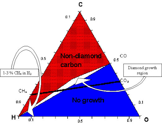
Figure 2.4. Triangular diagram of Bachmann
A further H abstraction
process on one of the chemisorbed groups creates a radical, which attacks the
other nearby carbon group to complete the ring structure, locking the two
carbons into the diamond lattice.
Diamond growth can be
considered to be a stepwise addition of carbon atoms to the existing diamond
lattice, catalysed by the presence of excess atomic H. In oxygen-containing
systems, it is believed that the OH radical plays a similar role to atomic H,
except that it is more effective at removing graphitic carbon, leading to
higher growth rates and better quality films.
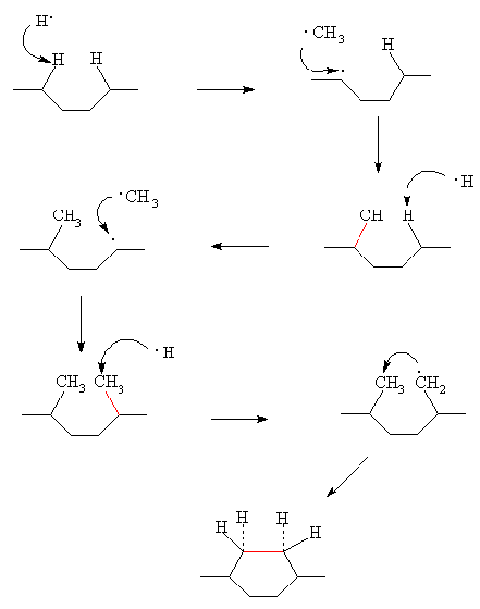
Figure
2.5. Schematic diagram of the diamond growth mechanism (in red colour the new
bonds formed)
2.1.9. Role of atomic hydrogen in the CVD growth
It has been proposed that atomic
hydrogen is the most critical component in the gas phase mixture, and indeed
that it drives the whole chemical system. In a hot filament system, atomic
hydrogen is produced heterogeneously by the thermal decomposition of H2.
A high concentration of atomic hydrogen is essential for a number of processes:
·
Although
the bulk of diamond is fully sp3 bonded, at the surface there is
effectively a “dangling bond”, which needs to be terminated in some way in
order to prevent cross-linkage, and subsequent reconstruction of the surface to
graphite. This surface termination is performed by hydrogen (or sometimes OH),
that keeps the sp3 diamond lattice stable. During the diamond
growth, some of these hydrogen atoms need to be removed and replaced by
carbon-containing species. A large number of reactive hydrogen atoms close to
the surface can quickly bond to any excess dangling bonds that may have been
created by thermal desorption or abstraction of the surface hydrogen atoms,
avoiding surface graphitization.
·
Atomic
hydrogen is known to etch graphitic sp2 carbon many times faster
than diamond-like sp3 carbon. The H atoms serve to remove back to
the gas phase any graphitic clusters that may form on the surface, while
leaving the diamond cluster behind. Diamond growth could be considered as “five
steps forward, but four steps back,” with the net result being a (slow)
build-up of diamond.
·
H
atoms are efficient scavengers of long-chained hydrocarbons, breaking them up
into smaller pieces. This avoids the build-up of polymers or large ring
structures in the gas phase, which might ultimately deposit onto the growing
surface and inhibit diamond growth.
·
H
atoms react with neutral species such as CH4 to create reactive
radicals, such as CH3·, which can attach to
adequate surface sites
2.1.10. In situ doping
The effects caused by
incorporation of dopants or impurities in CVD diamond films during the
deposition have been studied extensively during the last 10 years. This was
motivated first by the wish to make CVD diamond conducting in order to realise
electronic applications. Secondly by the more fundamental objective to study
the structural effects of dopants or impurities on the growth on CVD diamond
films.
The most common impurities
considered in diamond film technology are boron and nitrogen. Boron makes
diamond p-type with an activation energy of 0.37 eV. Nitrogen forms a deep
donor and is electrically inactive at room temperature. Its importance results
from its strong influence on the structural properties and the growth velocity
of the CVD diamond films 18. In order to realise n-type conductivity, several
other dopants such as lithium, sodium and phosphorous have been proposed 19. Koizumi et al.
20 reported on homoepitaxially grown CVD diamond films
doped with phosphorous which exhibit n-type conductivity with an activation
energy of 0.43 eV.
Normally, nitrogen can be
simply introduced to gaseous environment as N2 or NH3.
Boron, on the other hand, has to be added to the reactant gas in solid, liquid
or gaseous form. One commonly used gaseous form of boron at room temperature is
diborane. It has been used widely to dope CVD diamond films 21-24. However, diborane is highly toxic and for this
reason several less toxic and more easily handled sources in solid or liquid
form have been investigated. Solid sources used for boron doping include boron
powder 25 and boron trioxide (B2O3) 26. Boric acid (H3BO3) 27, cyclic organic borinate ester 26 and trimethylborate ((CH3)3BO3)
27 are liquid sources which have been applied
successfully.
The non-gaseous boron sources must be either heated or dissolved
in a high-pressure liquid, e.g. alcohol, to increase their vapour pressure
sufficiently. In order to control the boron concentration in the reactant gas,
bubbler systems have been applied in the case of boron trioxide dissolved in
alcohol, cyclic organic borinate ester and trimethylborate. Solid boron sources
have also often been placed near the substrate and heated until they can
diffuse to the growth surface.
The boron incorporation
depends on the texture of the diamond film or the orientation of the
single-crystal diamond. In single-crystal diamonds, Spytsin et al. 10 observed enhanced boron incorporation in (111)
diamond crystals. This result was confirmed by Samlenski et al. 28 who applied nuclear reaction analysis in order to
quantify the concentration of boron in doped homoepitaxial films. They found
the boron incorporation probability in (111) oriented films to be one order of
magnitude higher than in the (100) oriented films. Similar results were
obtained by Locher et al. 27 applying secondary ion mass spectroscopy on B-doped
polycrystalline CVD diamond with different textures. The total amount of boron
incorporated into CVD diamond films can be varied over several orders of
magnitude up to concentrations of about 1021 cm-3 without
significant deterioration of the structural quality under appropriate
deposition conditions. Whereas the probability for boron incorporation can be
higher than 10-1, the nitrogen incorporation probability was found
to be only about 5´10-4, dependent
also on the growth direction 28. However, under specific deposition conditions
nitrogen has a dramatic influence on the morphology and the structure of CVD
diamond films 29, 30.
2.1.11. Ex situ doping
Ex situ doping of diamond
can be performed by diffusion or ion-implantation. Diffusion of impurities in
diamond requires extremely high temperatures due to the low diffusion
coefficient at moderate temperatures. Successful boron doping by diffusion was
reported by Tsai et al. 31 for the fabrication of a diamond metal-semiconductor
field-effect transitor (MESFET).
Ion implantation is the
method of choice for modern microelectronics in silicon technology. However,
implantation requires annealing to remove the damage and to electrically
activate the implants. In this case diamond behaves quite differently than
silicon. Misleading results for diamond can be obtained due to the electrical
activity or damage in diamond caused by graphitization, amorphization or point-defect
agglomerates.
For implantation energies
from tens to hundreds of keV the penetration of energetic ions in the diamond
lattice creates mainly vacancies and interstitial carbon atoms. Fontaine 32 characterized boron implanted CVD diamond by electron
spin resonance and observed that below a dose threshold around 3´1015 B cm-2 the spin
number increased linearly with the ion dose and saturated above this threshold.
Assuming that spins originate from dangling carbon bonds, which leave paramagnetic
unpaired electrons, the defect formation rate was estimated to be 36 defects
per implanted ion. For doses above the threshold the defect concentration was
estimated to be in the order of 1021 cm-3.
2.1.12. Summary
A review about the
fundamental aspects of the diamond growth has been completed. In parallel the
influence of the substrate, different gas mixtures, temperature and pressure on
the growth process and growth mechanism have been discussed. In addition the
role of the hydrogen in the growth of diamond films have been described.
Finally some doping techniques to obtain low electrical resistance diamond have
been explained.
2.2. Diamond
Growth
The diamond samples of this thesis were provided by
Dr. M. Latto and Dr. P. May. The information details the growth they have
employed.
2.2.1. Introduction
Polycrystalline diamond possesses physical properties that suggest that electrodes fabricated from suitably doped samples of this material will exhibit advantageous attributes. For example, Compton and co-workers 33-39 have shown that in sonoelectrochemical experiments diamond electrodes are resistive to surface damage. In addition it has been claimed that boron doped diamond electrodes possess advantageous electrochemical characteristics that include: a wide potential window, low background currents and excellent resistance to surface fouling (cross-references section 1.5).
Therefore it is necessary to design and build a system capable of growing diamond in the adequate conditions to obtain the desirable material with the requirements cited before.
A scheme of the elements and gas lines that constitute the system employed to grow diamond in this study is displayed in Figure 2.6.
The elements of the system
will be described in the forthcoming sections.
2.2.2. Gas Flow System
Hydrogen (H2),
methane (CH4) and diborane (B2H6) gases (BOC
Speciality Gases) were used in the growth process.
Laboratory standard “high
purity hydrogen” and methane were used. The purities of the hydrogen and
methane were 99.995 (as “N4.5”) and 99.5% (as “N2.5”) respectively.
Diborane was supplied as a
4.75 % premix of diborane in hydrogen. Diborane is highly toxic, reactive and
explosive gas. Therefore special care was taken to ensure that all gas lines
were free of leaks (gas lines were leak tested several times before use). The
gas cylinder, the dilution cylinder and the associated piping were kept in a
specially designed fume cupboard to provide extra protection in case of an
accident. The reactivity of diborane made it necessary to avoid the use of many
materials including brass and nitrile rubber.
The source gases were stored
in gas cylinders with nominal pressures up to 200 bar at 15ºC. Regulators reduced the cylinder pressures to
the level of 1-2 bar above atmospheric pressure. Mass flow controllers fixed
the flow rates into a gas manifold where the gases were mixed before they
flowed along a common gas line into the reaction chamber.
The regulator on the
diborane gas cylinder was a stainless steel single stage design which could be
pumped down to vacuum and contained a purge line. This also allowed the
dilution procedure to be performed. The hydrogen and methane gas cylinders used
standard single brass regulators.
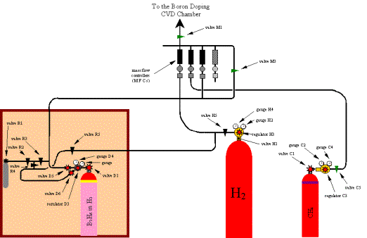
Figure
2.6. A schematic diagram of the gas lines which fed the diamond CVD chamber
2.2.3. Mass Flow Controllers
Three mass flow controllers
(MFC) were used to adjust the flow rate of each gas. Each MFC fixed the flow of
gas through a gas line and into a manifold where the gases were mixed (see
table 2.1).
The MFCs were controlled
electronically and could be programmed to allow a wide range of flow rates
through the gas lines. Two different MFC models were used to control diborane
gas flow rates in order to achieve low or high doping levels.
A bypass line was fitted
parallel to the MFCs to facilitate the pumping down of the diborane gas line.
There was the possibility of
adding a fourth MFC for bringing a new gas into the mixture. H2S, NH4
were proposed as an alternative doping source but this facility was not explored
in this study.
|
MFC number |
Gas |
Calibration |
Range (s.c.c.m) |
Conversion Factor |
|
1 |
Hydrogen (H2) |
Hydrogen |
0-200 |
1 |
|
2 |
Methane (CH4) |
Nitrogen |
0.0-10.0 |
|
|
3 |
Diborane (B2H6) in a carrier gas of
hydrogen (H2) |
Hydrogen (the main component of the mixture) |
0.0-10.0 or 0.00-1.00 |
1 |
|
4 |
Not used |
|
|
|
Table 2.1. Specifications of the mass flow
controllers.
2.2.4. Dilution
Diborane was supplied as
mixture of 4.75% B2H6 in H2. This amount of
diborane was too high for low doping and a dilution system was necessary to
decrease the concentration. This process could be repeated as many times as
necessary until the required concentration of B2H6 in H2
was reached.
A lecture bottle (capacity
0.4 dm3) was used as the mixing vessel. When B2H6
was diluted, this lecture bottle was used as the reservoir of B2H6
allowing a fixed flow rate of diborane in hydrogen for several hours.
A picture of the dilution
set-up could be seen in figure 2.7.
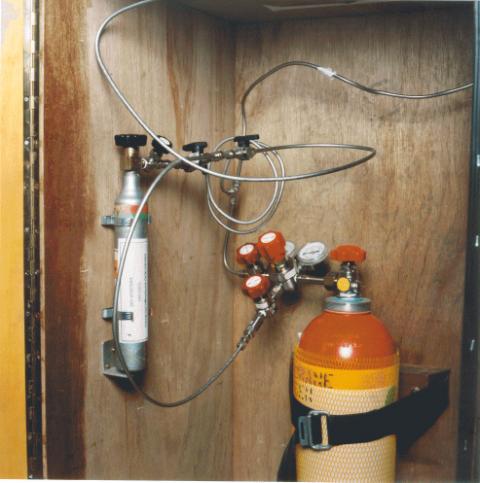
Figure 2.7. A picture of diborane dilution system
2.2.5. Deposition chamber
The deposition chamber
consisted of a single-walled stainless steel six-way cross with welded joints
and bolted flanges (see figure 2.8).
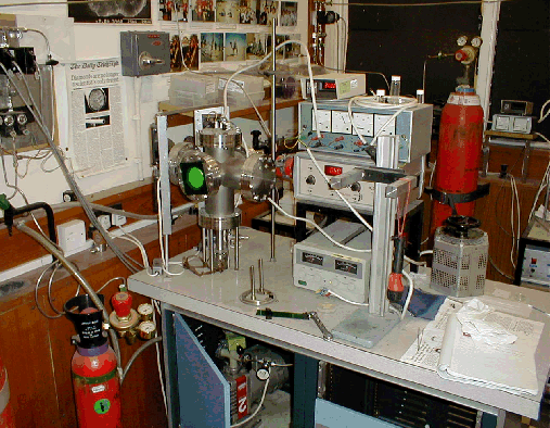
Figure 2.8. Hot filament CVD chamber
The deposition chamber could be divided in the next different
parts:
-
Top
flange.
-
Front
flange.
-
Bottom
flange.
-
Rear
flange.
-
Left
flange.
-
Right
flange
2.2.5.1. Top flange
This top flange contains the
following elements:
· Three
pairs of electrical contacts made from tungsten rods.
- One pair was used to supply power to
heat the substrate.
- The other to supply power to the
filaments.
-
Earthing
was achieved by a cable attached to this flange.
· Filament holder and substrate heater were attached
underneath the flange to allow new filaments and substrates to be loaded when
this flange was removed.
Two different insulation
processes were done in the top flange:
- Electrical insulation was performed
by glass coating.
- Vacuum sealing was
achieved by silicon rubber and epoxy resins.
2.2.5.2. Front flange
Front flange was
built with a glass window to allow visual monitoring of the growth process.
2.2.5.3. Bottom flange
The bottom flange was
connect to a two stage rotary pump via two stainless steel gas lines:
· A narrow bore line fitted with a needle valve allowed an accurate
control of the pressure inside the chamber during the growing process.
· A broad bore line was used to reduce as much as possible
the period of time to pump down the chamber.
Openings of these lines were
protected by copper gauze.
The exhaust line from the
rotary pump was guided to a vent.
2.2.5.4. Rear flange
Three gas lines fed into the
CVD chamber through this flange (see figure 2.9):
· Reaction
gas inlet leading from the mixing manifold.
· A connection to a pressure gauge (baratron) which was used
to measure the pressure in the chamber during the reaction.
· An air vent valve that allowed the chamber to reach
atmospheric pressure before it was opened
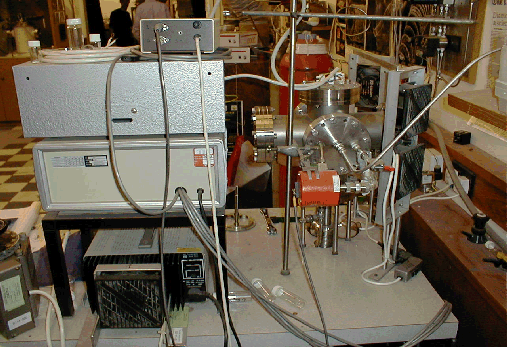
Figure 2.9. Rear view of the hot filament CVD chamber.
2.2.5.5. Left flange
No elements are
attached to this flange
2.2.5.6. Right flange
Right flange was
provided with two additional electrical contacts.
2.2.6. Substrate heater
2.2.6.1. Construction of the substrate heater
A nickel-chromium wire (24 SWG, standard gauge) was protected with insulating ceramic beads and coiled. Next, everything was covered by fire cement and heated until cement was dried. A molybdenum plate was placed onto the top of the cement block to yield a flat surface where samples could be placed. Molybdenum was chosen because of its properties: high melting point, inert in the reaction environment and uniform distribution of the heat across the plate.
Electrical connection
between the heating block and the tungsten feed-through were made with standard
copper flex insulated by ceramic beads (see figure 2.10).
2.2.6.2. Operating with the
substrate heater
An Iso-tech DC power supply
was used for the substrate heater. This was protected from overheating by an
external fan fitted behind the heat exchanger at the rear of the unit.
Substrate heaters were
operated by passing a current of 4 A through the Ni-Cr wire. To reach this
current it was necessary to apply a potential between 15 to 20 V. This wide
range of potential was dependent on the length of the Ni-Cr wire. Using these
parameters and comparing with the literature, it suggests a maximum heater
temperature of approximately 2400ºC.
The temperature was limited
by the cement which brokedown at approximately 1000ºC. Before the breakdown of
the cement vapour occluded from the pores of the cement burning the filament
and contaminating the chamber.
2.2.6.3. Maintenance
The substrate heater had an
average lifetime around 800 hours, after that the wires were very rigid and
brittle. At this stage they were very easily damaged.
The periodic replacement
avoided one of the sources of boron contamination, the pores of the cement
where boron was stored. The heater block could not be cleaned of this
contamination the only way of “cleaning” was the replacement of the heater block
at regular time periods.
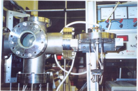
Figure 2.10. After a deposition run could be observed the structure of the substrate heater and a filament
2.2.7. Filaments
2.2.7.1. Construction of the filament
Filaments were formed using
tantalum wire (0.25 mm of diameter) coiled around a 4 mm rod. It was found that
ten turns of wire spanning 2 cm was the optimal geometry for the growing
process. Larger wires sagged producing a poor growth and in some cases damaging
the sample surface due to contact.
The chamber was equipped
with two filaments, connected in series, to allow large area growth or the
possibility of using more than one substrate per run.
When operating the chamber
in single filament mode there was the option of a simple rewiring to employ the
free filament if the first filament failed during the process.
The tantalum wire (Aldrich)
used had a purity of greater than 99.9%, the levels of impurity are listed in
the table 2.2
|
Element |
concentration (p.p.m.) |
|
Aluminium, Al |
120 |
|
Copper, Cu |
85 |
|
Tin, Sn |
80 |
|
Nickel, Ni |
35 |
|
Chromium, Cr |
20 |
|
Vanadium, V |
15 |
|
Magnesium, Mg |
1 |
Table 2.2. Trace elements in the tantalum wire
Values taken from
Supplier’s Certificate of Analysis
2.2.7.2. Operating conditions
The filaments were attached
to tungsten rods by stainless steel clamps and the power supply has provided by
a Variac variable resistor with an external voltmeter and amperometer. The
current was maintained at 6.75 A during the whole process.
Low-pressure conditions
could not be reached as they could have resulted in tantalum sputtering.
Under growth conditions,
tantalum filaments were carburised increasing their resistance and
necessitating an increase in the potential from the initial 20 V to 30V at the
end of the run (see figure 2.11).
After each run the filaments
were very brittle and were replaced before a new growth process was started.

Figure 2.11. The picture was obtained using an
infrared filter through the glass window during the growing process. It could
be observed the filament, substrate and heat substrate.
2.2.8. Substrates
2.2.8.1. Main features of the substrates
Silicon (Si) was the main
substrate for growing diamond for electrochemical characterisation. For studies
using diamond heat sinks the material was grown on quartz substrates.
The surface area of the
substrates was variable between 1 cm2 (1 cm ´ 1 cm) to
4 cm2 (2 cm ´ 2 cm). Typical was 2 cm2
(2 cm ´ 1 cm) because this allowed
two samples to be placed in the chamber at the same time giving a better yield
in the synthesis process. As the samples have been grown under the same
conditions, later electrochemical characterisation will allow better
experimental comparison.
The samples were prepared by
cutting pieces of silicon from silicon wafers supplied from the microchip
fabrication industry. The thickness of these wafers varied from 0.5 mm to 3 mm.
Quartz samples were already cut from the supplier in samples of 1 cm2
(1 cm ´ 1 cm) and 1 mm thick.
2.2.8.2. Pre-treatment of silicon surface before growing
The pre-treatment of silicon surface before growing was as follows:
1.
Abrasion of silicon surface. Samples were rubbed with
diamond powder (2-3 mm).
2.
Cleaning diamond waste. Diamond grit waste was
removed with 2-propanol
(IPA) soaked
cotton sticks.
3. Ultrasonic bath. Samples were finally treated in IPA ultrasonic bath for 15 minutes to remove very small diamond powder or possible impurities of the silicon.
2.2.9. Electrical contacts
Different types of electrical contacts have been used on the boron doped polycrystalline diamond samples during this study:
·
Indium/Gallium
eutectic contact
·
Silver
loaded epoxy resin contact
·
Three
layers (titanium/platinum/gold) metal contact
·
Titanium
under layer contact
Further details about the
electrical contacts can be found in chapter 3.
2.2.10. Typical growth conditions
Table 2.3 summarises the
typical growth conditions for the diamond films and appendix A gives full
details of the growth conditions for the films used in these studies.
|
Pressure |
20 Torr
|
|
Hydrogen flow rate |
200 s.c.c.m |
|
Methane flow rate |
1.4 s.c.c.m. |
|
Diborane flow rate (range) |
5 ´ 10-6 s.c.c.m. to 5 ´ 10-2 s.c.c.m |
|
Diborane flow rate (typical of low end) |
4 ´ 10-5 s.c.c.m |
|
Substrate temperature |
900 ºC |
|
Filament temperature |
2400 ºC |
|
Filament/substrate separation |
4 mm |
|
Deposition Time |
7 hours to 27 hours |
|
Substrates |
Si |
|
Filaments |
two ten-turn Ta coils |
Table 2.3. Typical deposition conditions for the hot-filament CVD reactor
2.3. Diamond
Characterization
2.3.1. Analytical techniques to characterize CVD diamond films
Material characterisation in
CVD diamond has been vital in sustaining progress in its development,
especially in recent years. Nowadays, there is easy access to highly efficient,
fast and extremely sensitive analytical tools to distinguish diamond from any
other forms of non-diamond carbon. Such tools include X-ray photoelectron
spectroscopy (XPS), X-ray diffraction, low energy electron diffraction (LEED),
electron energy loss spectroscopy (EELS), secondary ion mass spectrometry
(SIMS), and transmission electron microscopy (TEM). Secondary ion mass
spectroscopy (SIMS) cannot distinguish between the different forms of carbon
but is useful as a means to obtain a spatial distribution of different elements
that may be present within a few atomic layers of a surface. The two
characterisation methods mainly used in the present work to characterise the
samples provided by Dr. M. Latto and Dr. P. May are discussed in the next
sections: scanning electron microscopy and laser Raman spectroscopy.
2.3.1.1. Scanning Electron Microscopy
Scanning Electron Microscopy
(SEM) is a powerful tool for the examination of bulk specimens. Electrons are
generated by thermionic emission from a tungsten filament heated to
temperatures approaching 3000ºC. These are then focused onto the sample
surface. A detector then collects secondary electrons emitted from the surface
of the specimen. An image is then formed on a cathode-ray tube (CRT) display.
The SEM pictures were recorded on a Hitachi Model
3200 Scanning Electron Microscope operating with an accelerating potential of
25 keV. A Mamiya camera loaded with rolls of 6 ´ 7 cm film was used to
capture images. Other SEM studies were made in a JEOL JSM 5600LV Scanning
Electron Microscope. This second SEM machine had digital image rather than a
conventional camera, allowing more flexible treatments for the SEM
pictures.
SEM requires samples that
are electrically conductive. In order to increase the surface conductivity of
insulating samples, a layer of gold (Au) was deposited with an Edwards S150A
Sputter Coater. This treatment was not required for the boron doped diamond
samples as the doping made them sufficiently conductive.
Inspection of the SEM
micrographs can provide valuable information on the topology of the diamond
films:
·
Top
view. The average grain size as well as the surface morphology of the deposited
films
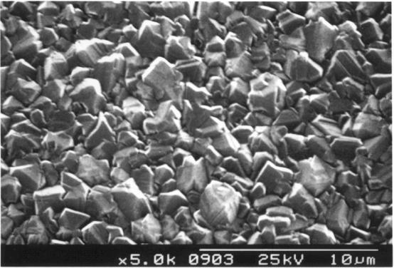
Figure 2.12. Randomly oriented HFCVD diamond film (sample B141a)
·
Cross-sectional
View. The film thickness and roughness
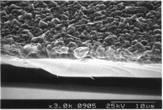
Figure 2.13. Cross-section SEM picture of a thin diamond film
However, such
images, in themselves, do not prove whether the films are diamond.
Additional SEM pictures can
be seen in the next pages:
Figures 2.14 to 2.16 shows
SEM images of a diamond sample using different resolutions. The size, quality
and morphology of the diamond crystals in the film can be estimated.
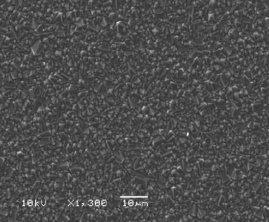
Figure 2.14. A continuous HFCVD diamond film. (Sample B117)
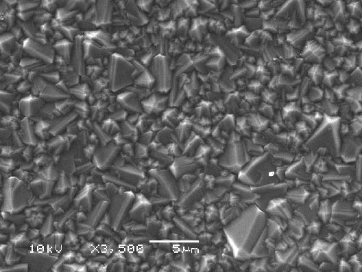
Figure 2.15. A continuous HFCVD diamond film. (Sample B117)
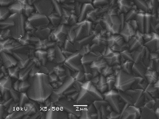
Figure 2.16. A continuous HFCVD diamond film. (Sample B117)
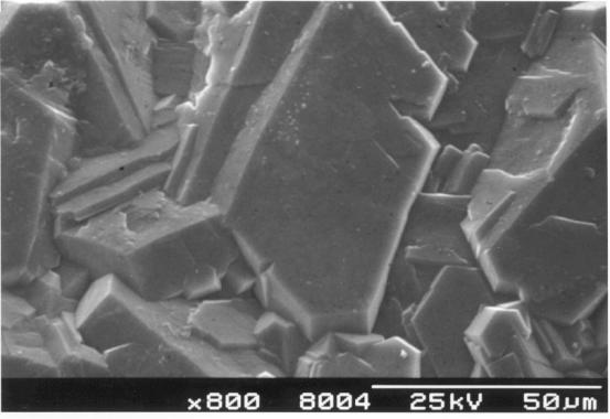
Figures 2.17 to 2.19 show
SEM images of a sample where the diamond growth had been stopped after 5 hours
and 35 minutes. Figure 2.17 shows the surface morphology at the centre of the
sample where the diamond film was continuous and well defined facets. Figures
2.18 and 2.19 show the surface morphology at the edges of the sample where the
growth had not progressed far beyond the nucleation stage, leaving individual
crystals on the silicon substrate.
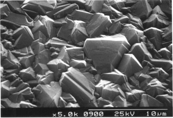
Figure 2.17. A continuous diamond film with well defined facets. (Sample B142a)
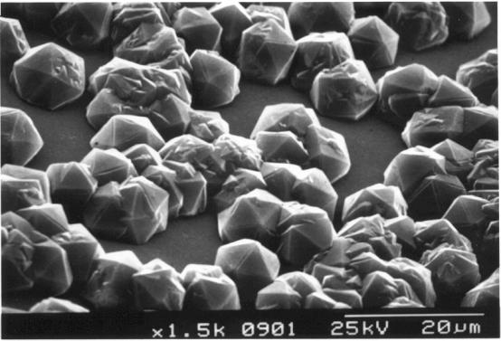
Figure 2.18. Incomplete surface coverage at the edge of a thin diamond film. The silicon substrate is visible behind the diamond crystals. (Sample B142a)
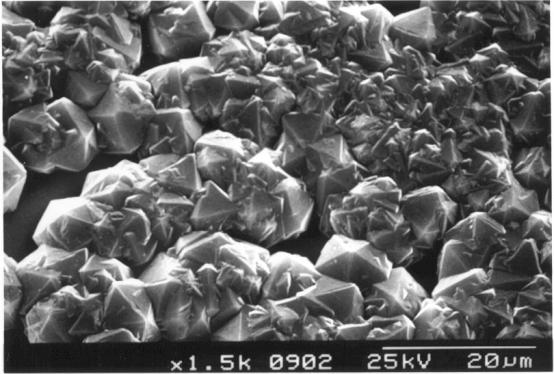
Figure 2.19. The reaction was stopped at the stage where the individual crystals have started to coalesce to form a continuous film. (Sample B142a)
The quality and morphology
of the films was comparable to the same one in the industrial grown samples.
Figures 2.20 to 2.22 show an industrial free-standing diamond film that was
grown for an optical application in the aerospace industry using microwave
plasma assisted CVD (MPACVD) 40. The industrial film was grown continuously for ten
days yields a much thicker sample (175 mm) than the HFCVD diamond
films. It shows lager facet sizes (approximately 50 mm)
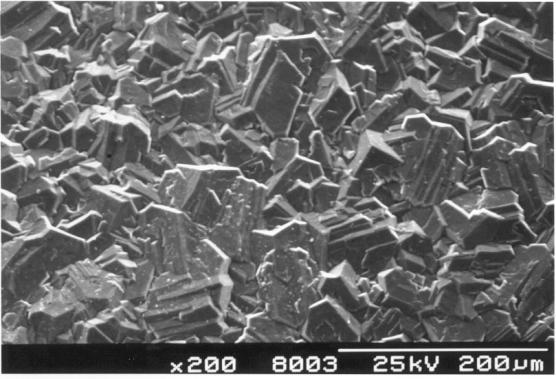
Figure 2.20. Industrial undoped MPACVD diamond
Figure
2.21. Industrial undoped MPACVD diamond.

Figure 2.22. A cross-section of a free-standing industrial undoped MPACVD diamond.
Figures 2.23 and 2.24 show
two different samples grown on quartz substrate. The quality and morphology of the
films was comparable to same one in the silicon substrate samples.
Figure 2.23. Randomly orientated undoped diamond sample on quartz substrate (sample Q1)
During the cooling stage of
the diamond sample if the quartz substrate contracts in a non-homogeneous
process the result could be the cracking of the diamond film (see figure 2.25).
Other side effect could be the appearance of pinholes in the diamond structure
(see figure 2.26)

Figure 2.24. Randomly orientated undoped diamond sample on quartz substrate (sample Q2)

Figure 2.25. Crack undoped diamond film on quartz substrate (sample Q3).
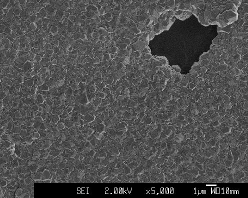
Figure 2.26. Pinhole in the undoped diamond structure grown on quartz substrate (sample Q3)
2.3.1.2. Laser Raman Spectroscopy
Laser Raman Spectroscopy
(LRS) is the most widely used technique to identify the characteristic energies
of the chemical bonds or to distinguish between different phases within the
same material. For this reason it is a decisive tool for establishing that the
film is indeed diamond and for providing some measure of the film quality. The
Raman effect is an interaction between monochromatic light, such as from a
laser source, and the chemical bonds within a specimen. Thus when the laser is
irradiated on the specimen, a small number of photons may excite molecular
vibrations in the specimen. Consequently, these photons will be scattered with
a slightly lower energy.
Raman spectra were taken
with a Renishaw Raman Imaging Microscope and Spectrometer with a spectral
resolution of 1 cm-1. An argon gas laser with a wavelength of 488 nm
(green light) was used to provider the incident laser beam.
The Raman spectrum of
natural diamond shows a sharp, single peak centred at a wavenumber of approximately
1332 cm-1. This feature also dominates the Raman spectra of high
quality, polycrystalline diamond film grown by CVD methods. However, additional
peaks may be observed in the spectra which are characteristic of non-diamond
contamination, depending on the deposition conditions (such as films grow with
high methane concentration in gas phase). The Raman spectrum of graphite shows
a broad feature centred on 1580 cm-1. When characterising CVD
diamond films, the observation of any broad resonance at higher wavenumber is
generally taken to indicate the presence of graphite-like non-diamond phases
containing sp2-bonded carbon atoms.
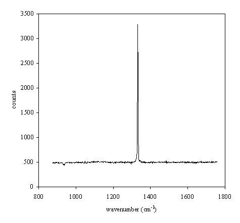
Figure 2.27. Raman spectrum of a type IIbª natural diamond.
The full width half maximum
(FWHM) of the 1332 cm-1 Raman line is another measure of film
quality; good quality CVD diamond films normally produces peaks with a FWHM of
4-10 cm-1, whilst linewidths close to those natural diamond if the
films are non-continuous, giving rise to separate diamond crystals.
Some of the Raman spectra of the diamond samples used in this study are presented here:
Sample b140a presents a
shoulder band about 1550 cm-1 indicating the weak presence of
graphite.
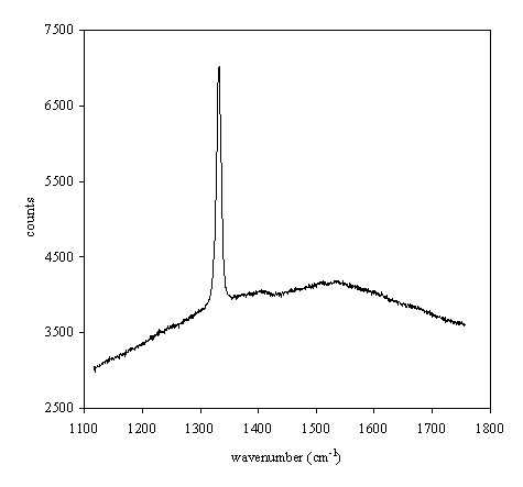
Figure 2.28. Raman spectrum of boron doped diamond film
(B140a)
Sample b140b no presents a
shoulder band about 1550 cm-1 such as b140a sample, indicating that
graphite is almost neglectled.
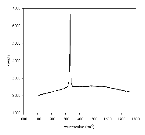
Figure 2.29. Raman spectrum of boron doped diamond
film (B140b)
Sample Q1 (undoped diamond grown on quartz substrate) presents a shoulder band about 1550 cm-1 indicating the weak presence of graphite when is compared against the sharp peak for approximately 1333 cm-1 (see figure 2.30).
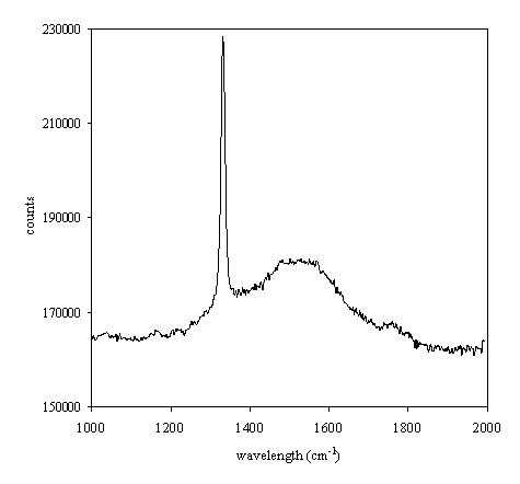
Figure 2.30. Raman spectrum of undoped diamond film grown on quartz substrate (Q1).
2.4. Summary
The system employed to grow
the diamond samples used in these studies has been explained in detail.
Furthermore analytical techniques used in the identification and
characterisation of the diamond samples have been presented. Results were
discussed. Good quality undoped and boron doped diamond samples have been
achieved.
2.5. References
1 S. Tennant, Phil. Trans. R. Soc. Lond. A, 1797, 87, 123.
2 F. P. Bundy, J. Geophys. Res., 1980, 85, 6930.
3 J. E. Field, 'The properties
of natural and synthetic diamond', ed. Academic, 1992.
4 F. P. Bundy, H. T. Hall, H.
M. Strong, and R. H. Wentforf, Nature,
1955, 176, 51.
5 W. G. Eversole, US Patent
nos 3030187, 3030188, 1958.
6 B. V. Deryagin, D. V.
Fedoseev, V. M. Lukyanovich, B. V. Spitsyn, A. V. Ryanov, and A. V. Lavrentyev,
J. Cryst. Growth, 1968, 2, 380.
7 J. C. Angus, H. C. Will, and
W. S. Stanko, J. Appl. Phys., 1968, 39, 2915.
8 D. J. Poferl, N. C. Gadner,
and J. C. Angus, J. Appl. Phys.,
1973, 44, 1418.
9 B. V. Deryagin, B. V.
Spytsyn, L. L. Builov, A. A. Klochov, A. E. Gorodetskii, and A. V. Smolyanimov,
Dokl. Akad. Nauk. SSSR, 1976, 231, 333.
10 B. V. Spytsin, L. L.
Bouilov, and B. V. Derjaguin, J. Cryst.
Growth, 1981, 52, 219.
11 S. Matsumoto, Y. Sato, M.
Tsutsumi, and N. Setaka, J. Mater. Sci.,
1982, 17, 3106.
12 S. Matsumoto, Y. Sato, M.
Kamo, and N. Setaka, Jpn. J. Appl. Phys.
Part 2 - Lett., 1982, 21, L183.
13 M. Kamo, Y. Sato, S.
Matsumoto, and N. Setaka, J. Cryst. Growth,
1983, 62, 642.
14 Y. Saito, S. Matsuda, and S.
Nogita, J. Mater. Sci. Lett., 1986, 5, 565.
15 P. W. May, N. M. Everitt, C.
G. Trevor, M. N. R. Ashfold, and K. N. Rosser, Appl.Surf. Sci., 1993, 68,
299.
16 D. G. Goodwin and J. E.
Butler, 'Handbook of industrial diamonds and diamond films', ed. M.A. Prelas,
G. Popovici, and L. K. Bigelow, 1997.
17 P. K. Bachmann, H. J.
Hagemann, H. Lade, D. Leers, F. Picht, D. U. Weichert, and H. Wilson, Mater. Res. Soc. Symp. Proc., 1994, 339, 267.
18 W. Muller-Serbet, E. Worner,
F. Fuchs, C. Wild, and P. Koidl, App.
Phys. Lett., 1996, 68, 759.
19 S. A. Kajihara, A.
Antonelli, J. Bemhole, and R. Car, Phys.
Rev. Lett., 1991, 66, 2010.
20 S. Koizumi, M. Kamo, Y.
Sato, H. Ozaki, and T. Inuzuka, App.
Phys. Lett., 1997, 71, 1065.
21 N. Fujimori, H. Nakahata,
and T. Imai, Japan J. Appl. Phys.,
1990, 29, 824.
22 K. Miyata, K. Kumagai, K.
Nishimura, and K. Kobashi, J. Mat. Res.,
1993, 8, 2845.
23 J. Mort, D. Kuhman, M.
Machonkin, M. Morgan, F. Jansen, K. Okumura, Y. M. LeGrice, and R. J. Nemanich,
App Phys Lett, 1989, 55, 1121.
24 H. Shiomi, Y. Nishibayashi,
N. Fujimori, and K. Kobashi, Japan J.
Appl. Phys., 1991, 30, 1363.
25 S. A. Grot, C. W. Hartfield,
G. S. Gildenblat, A. R. Badzian, and T. Badzian, App. Phys. Lett., 1991, 58,
1542.
26 X. K. Zhang, J. G. Guo, Y.
F. Yao, R. Wang, G. M. Chen, W. K. Zhou, and S. Yu, Appl. Phys. A, 1993, 56,
425.
27 R. Locher, J. Wagner, F.
Fuchs, M. Maier, P. Gonon, and P. Koidl, Diam.
Relat. Mater., 1995, 4, 678.
28 R. Samlenski, C. Haug, R.
Brenn, C. Wild, R. Locher, and P. Koidl, Diam.
Relat. Mater., 1996, 5, 947.
29 R. Locher, C. Wild, N.
Herres, D. Behr, and P. Koidl, App Phys
Lett, 1994, 65, 34.
30 S. Jin and T. D. Moustakas, Appl. Phys. Lett., 1994, 65, 403.
31 W. Tsai, M. Delfino, D.
Hodul, M. Riazat, L. Y. Ching, G. Reynolds, and C. P. Cooper, IEEE Electron Device Lett., 1991, 13, 126.
32 F. Fontaine, 'Doping of
diamond by ion implantation', Unpublished review, 1997.
33 R. G. Compton, F. Marken, C.
H. Goeting, R. A. J. McKeown, J. S. Foord, G. Scarsbrook, R. S. Sussman, and A.
J. Whitehead, Chem. Commun., 1998,
1961.
34 C. H. Goeting, F. Marken, R.
G. Compton and J. S. Foord, Chem. Commun.,
1999, 17, 1697.
35 C. H. Goeting, J. S. Foord,
F. Marken, and R. G. Compton, Diam.
Relat. Mater., 1999, 9, 824.
36 K. B. Holt, J. Del Campo, J.
S. Foord, R. G. Compton, and F. Marken, J.
Electroanal. Chem. , 2001, 513,
94.
37 A. J. Saterlay, S. J.
Wilkins, C. H. Goeting, J. S. Foord, R. G. Compton, and F. Marken, J. Solid State Electrochem., 2000, 4, 383.
38 A. J. Saterlay, S. J.
Wilkins, K. B. Holt, J. S. Foord, R. G. Compton, and F. Marken, J. Electrochem. Soc. , 2001, 148, E66.
39 J. D. Wadhawan, F. J. Del
Campo, R. G. Compton, J. S. Foord, F. Marken, S. D. Bull, S. G. Davies, D. J.
Walton, and S. Riley, J. Electroanal.
Chem., 2001, 507, 135.
40 D. A. Tossell, M. C.
Costello, A. P. Webb and K. C. Vanner, Pure
and Appl. Chem., 1994, 66, 1335.
41 W. J. P. Van Enckevort, 'Physical,
chemical and microstructural characterisation and properties of diamond in synthetic
diamond: emerging CVD science and technology', ed. K. P. Spear and J. P.
Dismukes, J. Wiley and sons Inc., 1994.