Chapter 3
Electrical contacts to semiconducting diamond
3.1. Introduction
For electrochemical studies
an ohmic contact is required. An ohmic contact is considered as one that does
not add a significant parasitic impedance to the structure and does not
sufficiently change the equilibrium carrier concentration within the
semiconductor or affect the device characteristics. In other words, an ohmic
contact should have linear and symmetrical current-voltage relationship; it is
characterized by having no potential barrier (hence no asymmetry) and an
infinite surface recombination velocity (hence linearity). At an ohmic contact
the electron and holes are at their thermal equilibrium values 1.
In practice, the above definition
is valid only for an ideal situation. In reality all the requirements should be
taken in a much more approximate manner. Moazed et al. 2, 3 suggest that a contact is ohmic if the potential drop
across it is small compared to that across the active portion of the device.
To obtain an ohmic contact
one can match the metal work function (f) to the bands of the
semiconductor. Alternatively one can decrease the electron affinity (c) of the semiconductor. In the case of
diamond (see below) this is achieved by altering the surface termination.
Despite of the high number
of studies published on the electrochemistry of highly boron doped diamond
samples 4-15 only a few consider the Ohmic contact 16-20. This study shows different types of electric
contacts generally used for boron doped polycrystalline diamond devices.
Properties and applications are discussed. A new ohmic metal-semiconductor
contact not described in the polycrystalline diamond electrochemistry
literature is presented.
3.2. Indium/Gallium Eutectic Electrical Contacts
Indium/Gallium (In/Ga)
eutectic is extensively used to make electrical contacts in silicon technology 1. Also this method can be found as a procedure in the
early stages of the diamond technology development 21.
This section describes how
to build the electrical contact and discusses the doping range over which its
application is useful.
3.2.1. Construction of the electrical contact
The boron doped diamond substrate
(conductive silicon) backside was scratched with a diamond scribe. The In/Ga
eutectic was deposited on the silicon and a steel strip pressed onto the liquid
eutectic. To protect the contact, the sample and metal strip were covered using
a PTFE (polytetrafluoroethene, (C2F2)n) tape
(very resistant against acids, bases and strong oxidising agents), leaving
exposed only the area on which to perform the electrochemical experiments.
Silicon substrate samples had to be doped (n-type)
and dipped in a hydrofluoric acid (HF) solutionª (just a few seconds) to
remove any possible insulation layer of SiO2 and rinsed in 18.2 MW cm ultrapure deionised
water (Millipore) immediately prior to the contact formation.
3.2.2. Results
This type of contact was
used successfully for highly doped diamond samples ([C]/[B] ratio of 2.8´104 to 3.0´104 p.p.m in the gas phase).
A poor performance for low
boron doped diamond samples was found.
This technique was limited by the need to consider the effects of the liquid contact and interface between the silicon and the diamond.
3.2.3. Conclusions
The Ga/In eutectic contact
was successful for highly conductive films but was limited by the need to use
HF solutions and the poorly characterised interface between the silicon and the
diamond.
Due to these limitations the
technique was abandoned in favour of a simple technique: silver loaded epoxy
resin electrical contacts.
3.3. Silver Loaded Epoxy Resin Electrical Contacts
Silver loaded epoxy resin
electrical contacts have been used extensively as a general procedure for
contacting boron doped polycrystalline diamond in electrochemistry 6-8, 22-36.
A description of the
construction method is detailed in this section. Silver loaded epoxy resin
electrical contact is analysed using a simple technique such as current-voltage
(i-V) curves. The range of
application of this contact is considered in terms of the doping level of the
diamond sample.
3.3.1. Construction of the electrical contact
Contact was made by simply
applying silver loaded epoxy resin (“silver paint”) on a wire attached on top
of the diamond surface. The contact was protected using a layer of a strong
resin adhesive (Araldite Rapid) on top of the contact.
3.3.2 Results and discussion
Current-voltage (i-V)
curves were employed to determine the quality of the contacts. These were
recorded using a m-Autolab potentiostat (Eco
Chemie B.V.) in two-electrode configuration. The scan rate was 50 mV/s.
Figure 3.1 shows the i-V curve of an as grown sample with two silver paint contacts. The
concentration of boron in the gas phase during the growth of this diamond sample
was 3´103 ppm. The voltage range of the
experiment was from –5 V to 5 V. The
plot is symmetrical with linear region between –0.5 V and 0.5 V. The resistance
of the film calculated from the reciprocal of the slope in the linear region
was 475 W.
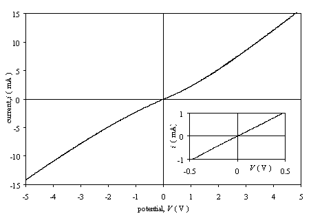
Figure
3.1. Current-voltage characteristics for an as-grown moderately doped diamond
film with two silver paint contacts (sample B111).
Figure 3.2 shows the i-V curve of an as grown sample with two silver paint contacts. The
doping level of this diamond was unknown because no doping source was used
during the growth just the boron contamination in the chamber. The experiment
was done in the same conditions as above. The plot is asymmetrical without any
linear region.
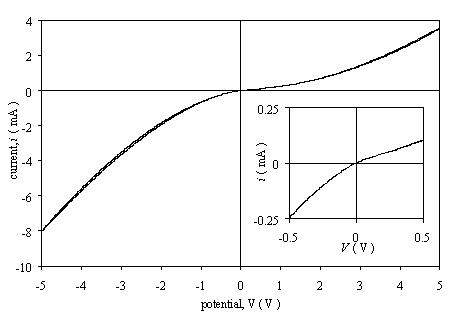
Figure
3.2. Current-voltage characteristics for an as-grown low doped diamond film
with two silver paint contacts (sample B112).
Silver paint could be
considered to yield ohmic contacts when used in samples with doping levels
([B]/[C] ration in gas phase) higher than 3´103 ppm and over
a narrow potential range. When silver paint was utilised for low doped diamond
samples no Ohmic contact was observed due to a Schottky barrier formed at
metal/semiconductor interface. (See figure 3.3).
This type of contact because
it was on top of the diamond surface reduced the space available for
electrochemical studies, causing difficulties when the dimensions of the sample
were small.
Silver paint contacts
eliminated the hazardous treatment of using HF solutions and simplified the
process. There were no restrictions in possible pre or post-treatments because
this contact was compatible with a range of surface treatment.
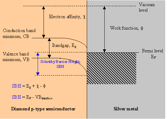
Figure 3.3. The metal/semiconductor interface
3.3.3. Conclusions
Successful contacts were made using silver paint in
high doped diamond samples ([C]/[B] ratio of 3´103 to 3.3´104 p.p.m.). Silver paint
electrical contact cannot be applied to low doped diamond samples because of
the Schottky barrier formed at the metal/semiconductor interface.
The simple procedure of construction and ease of pre or post-treatment
indicate that this contact is favourable for highly doped diamond samples.
3.4. Gold Electrical Contacts
In the literature it has
been reported that gold forms a Schottky barrier when deposited on
semiconducting diamond 37. However, this behaviour is rarely observed and Ohmic
contacts are more usually reported 38.
A description of the gold
electrical contact method is detailed in this section. Gold electrical contact
is analysed using the simple technique of current-voltage (i-V)
curves. The range of application of this contact with respect to doping level
of the diamond sample is discussed.
3.4.1. Construction of the electrical contact
Gold layers were deposited
using an Edwards evaporator which was modified to incorporate a heating stage
(further details are given in the next section: Formation of Three Metal Layers
Contacts).
To increase the adhesion of the
gold layer, samples were heated under vacuum to remove organic contaminants
from the surface. After this stage, gold was deposited on the clean surface.
The samples were cooled under vacuum.
The evaporator worked by passing a current through a tungsten three wire basket containing the metal (a ball of gold wire). A current of 30 A was enough to evaporate the gold stored in the basket. The diamond samples were covered with a mask to allow deposition in the shape of a circle (2 mm diameter) at the edge of the substrate. The distance between the holes and the mask was 1cm.
Gold was evaporated. When the metal started to cool down, gold vapour solidified and coated the inside of the evaporation chamber. Two gold spots were deposited on the diamond surface. The deposition of the metal was controlled to yield gold layers of approximately 100 nm in thickness.
Applying silver paint on a wire attached on top of the gold spot made the electrical contact. The contact was protected using a layer of a strong resin adhesive (Araldite Rapid) deposited on top of the contact.
Two pairs of diamond samples were grown. Each pair was grown in a single deposition run to minimise variation between the films. One sample from each pair was refluxed in chromic acid solution to oxidise the diamond surface, while the other sample remained “as grown”.
Samples B123a and B123b were grown with no boron in the gas phase, i.e. doping was achieved using that boron in the CVD chamber as contamination. Samples B128a and B128b were grown with a gas phase boron to carbon ratio of 50 ppm.
To remove contacts immersion in an aqua regia solution (1 HNO3: 3 HCl (aq)) was sufficient.
3.4.2. Results and discussion
Current-voltage (i-V) curves were employed to describe the quality of the contacts using a m-Autolab potentiostat (Eco Chemie B.V.) in two-electrode mode configuration. The scan rate was 50 mV/s.
Results showed an asymmetrical non-linear behaviour. The moderately doped samples (B128a and B128b) gave an approximately ohmic response over a reduced potential range (-0.5 V to +0.5 V) while the low doped samples (B123a and B123b) gave a non-linear answer for all the potential range of the i-V plots. (Figures 3.4 and 3.5)
It was believed that the reflux in chromic acid had successfully modified the hydrogen termination of the diamond surface. A simple test with ultrapure water showed the “as grown” sample to be hydrophobic and the oxidised sample to be hydrophilic.
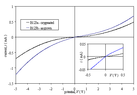
Figure 3.4. Current-voltage
characteristics for diamonds films with two gold contacts (sample B123a and
B123b).

Figure 3.5. Current-voltage characteristics for diamonds films with two gold contacts (sample B128a and B128b).
Gold electrical contact was limited by boron doping level of the diamond sample. When diamond samples were very low doped (hydrogen or oxygen terminated) a Schottky contact was described. But using moderately boron doped diamond samples the response of the gold contact was acceptable for a small range of potential. It should be noted that it was difficult to compare results because of the poor reproducibility of gold contact formation due to poor adhesion.
Poor adhesion of the gold layer was one of the biggest difficulties of this type of contact. Even if the diamond surface was cleaned either by chemical treatment (chromic acid) or by heating process. The gold did not adhere well on the diamond surface. Carefully handling of the diamond samples was a requirement after the gold deposition to avoid a possible delamination of the gold spots.
An advantage of this type of contact was that it did allow any kind of treatment of the diamond surface before the gold deposition.
As this type of contact was made on top of the diamond surface it reduced the available space causing difficulties when the dimensions of the samples were small.
3.4.3. Conclusions
An Ohmic response was found over a reduced applied potential range (-0.5 V to +0.5 V) for moderately boron doped samples. Poor performance was observed for low doped diamond.
Problems in the reproducibility when the contact was made complicate the analysis of the gold contact properties.
Gold contacts did not provide a significant improvement in performance over the simpler silver paint contact.
3.5. Three Layer Metal Electrical Contacts
Reaction at the interface to
produce a third phase is a useful method of changing the nature of metal
contacts on semiconductors (reduction of the Schottky barrier)39, 40. For diamond, the third phase formed is a carbide,
which could be a reliable contact as well as a good diffusion barrier for
high-temperature application. Annealing process (heating up the carbide forming
metal) promotes the formation of the carbide layer.
Carbide forming metals including
titanium, molybdenum, and tantalum have been used to obtain ohmic contact on
diamond. Collins, Lightwowlers, and Williams used a gold tantalum alloy 21. Titanium (Ti) has been used by several groups of
researchers and was often capped with platinum/gold (Pt/Au) overlayers 2, 3, 17, 18, 41. Various combinations of carbide forming refractory
metals have also been studied to obtain ohmic contacts of low resistivity 2,
3.
Titanium was selected as a metal
representing the carbide forming metals for the following reasons: titanium is
a transition metal which has a great affinity for carbon (carbide formation is
thermodynamically favourable, DH= - 44 kcal/mol at 25ºC);
it is estimated that the diffusion constant of carbon in titanium is orders of
magnitude higher than the other carbide forming metals 42.
In this section, Ti/Pt/Au (three layer metal, 3LM) contacts on
boron doped polycrystalline diamond are detailed. As the literature described
before, titanium was chosen as a metal representing the carbide forming metals
that could be annealed to produce titanium carbide (TiC). A gold top layer was
deposited to avoid the oxidation of titanium with traces of oxygen at high
temperature (during the annealing process) and, more slowly, over the lifetime
of the device. The presence of a third metal, platinum was required to prevent
the interdiffusion between titanium and gold layers during the annealing step.
Wires could be attached to
the surface of gold using silver paint, as was described before in the section
on gold contacts.
A description of the 3ML
electrical contact procedure is detailed in this section. 3ML electrical
contacts were analysed using simple techniques such as current-voltage (i-V) curves and four point probes
resistance measurements. The range of application of this contact is given in
terms of the doping level of the boron doped polycrystalline diamond sample.
3.5.1. Construction of the electrical contact
Before any metal was
deposited the diamond surface was oxidised and cleaned from any non-diamond
carbon. For this task, the sample was refluxed in a chromic acid solution at
100°C for a period of about 4 hours. After the
solution had cooled down, samples were rinsed with ultrapure water and dried in
an oven for approximately 1 hour.
When the diamond samples
were loaded into the evaporator (see figure 3.6), a heating treatment was
necessary to remove any physisorbed species from the diamond surface to enhance
adhesion prevent the oxidation of the metal. The samples were located in a
heating stage inside the vacuum chamber of the evaporator. A mask was placed on
top of the sample and a three-wire tungsten basket (Alfa Aesar) was loaded with
titanium crystals (Alfa Aesar). The masks were made from 0.5 mm thick stainless
steel contained circular holes
(diameter 2 mm; spacing 8mm).The vacuum chamber was insulated with the
bell jar and pumped down to less than 2´10-5 Torr.
Samples were heated between 200 °C and 250 °C. An alternating current between 40 A to 48
A was passed through the tungsten basket to evaporate the titanium crystals. A
layer of 100 nm to 150 nm of titanium was deposited at a rate of approximately
0.5 nm/min, monitored using a quartz crystal microbalance.
When the titanium deposition
was over, the sample was allowed to cool down to room temperature slowly under
vacuum. Normally this process was done
overnight. Although not employed in this study the cooling could be
accelerated using a flow of a dry oxygen-free gas.
To reach the desired
titanium thickness it was frequently necessary to use more than one run. The
loading, heating, deposition and cooling processes were repeated many times.
Once the titanium deposition
was complete a platinum layer was deposited. A 60 nm thick platinum layer was sputtered onto the titanium. A
mask was used with a 4 mm diameter spot a diameter greater than the one that
was used for the titanium deposition in order to ensure complete coverage of
the lower metal.
Gold deposition was
performed in the evaporator with an approximate thickness of 100 nm covering
the whole platinum spot. To ensure complete coverage a mask which the diameter
of the holes was 6 mm was employed.
After each step of the
process, the three metal layer structure was examined by the naked eye and with
an optical microscope to verify the alignment, coverage and quality of the
metal layers.
The final stage of the
process was annealing. Reviewing the literature data suggested that an
annealing process of 500 °C in vacuum would be
sufficient to form the titanium carbide layer 3.
Samples were loaded in a
quartz cell designed with two taps to allow evacuated and fluxed gases through
it. The annealing process was divided in two steps. The first part consisted of
pumping down the cell using a rotary pump. The cell was flushed with
oxygen-free nitrogen or helium (BOC Speciality Gases). The vessel was
frequently flushed with nitrogen to eliminate the oxygen before the oven was
switched on to heat up the cell to 250 °C. During this process the
cell was evacuated by a rotary pump to remove species as soon they desorbed
from the surface of the sample and the walls of the vessel. Whilst hot
(temperature about 250 °C), the cell was transferred
to a high temperature furnace for annealing at 500 °C once completed the cell was left to cool
down to room temperature. A schematic diagram about this contact can be found
in figure 3.7.
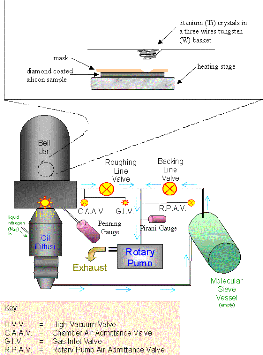
Figure 3.6. Schematic diagram of the metal evaporator
Next table (table 3.1)
offers a schematic resume of the 3LM contact production process.

Figure 3.7. Schematic diagram of a three layer metal
top contact (not to scale). Note that the plan view shows the metal layers in
reverse order for illustrative purposes. The layers from top to bottom are Ag,
Au, Pt and Ti.
Step
|
Description |
Step |
|
|
1 |
Nucleation
pre-treatment |
(a)
Abrade with diamond powder to provide nucleation sites |
1.a |
|
2 |
Removing
diamond dust |
(a)
Wipe with IPA soaked cotton sticks (b)
Place in a beaker of IPA in an ultrasonic bath |
2.a |
|
2.b |
|||
|
3 |
Diamond
growth |
(a)
Load substrate into chamber (b)
Evacuate chamber (c)
Pre-heat substrate (d)
Deposit diamond for several hours (e)
Initially cool in hydrogen atmosphere (f)
Reach room temperature under vacuum |
3.a |
|
3.b |
|||
|
3.c |
|||
|
3.d |
|||
|
3.e |
|||
|
3.f |
|||
|
4 |
Surface Pre-treatment |
(a)
Sample reflux in chromic acid solution (b)
Rinse sample with ultrapure water |
4.a |
|
4.b |
|||
|
5 |
Titanium
deposition |
(a)
Load samples into evaporator (b)
Load metal into the basket (c)
Place mask over the sample (d)
Evacuate chamber (e)
Heat sample to remove physisorbed species (f)
Evaporate titanium onto diamond surface (g)
Reach room
temperature under vacuum
(h) Repeat from 2nd step until obtain desired thickness |
5.a |
|
5.b |
|||
|
5.c |
|||
|
5.d |
|||
|
5.e |
|||
|
5.f |
|||
|
5.g |
|||
|
5.h |
|||
|
6 |
Platinum
deposition |
(a)
Load sample into the chamber (b)
Place mask over the sample (c)
Evacuate chamber (d)
Sputter platinum over the titanium spot |
6.a |
|
6.b |
|||
|
6.c |
|||
|
6.d |
|||
|
7 |
Gold
deposition |
(a)
Load sample into evaporator (b)
Place mask over sample (c)
Heat sample to eliminate physisorbed species (d)
Evaporate gold over platinum spot (e)
Reach room temperature under vacuum |
7.a |
|
7.b |
|||
|
7.c |
|||
|
7.d |
|||
|
7.e |
|||
|
8 |
Annealing
process |
(a)
Put samples into quartz cell (b)
Evacuate cell (c)
Flush cell with nitrogen (d)
Repeat steps 2 and 3 several times (e)
Evacuate cell (f)
Heat sample until 250 °C (g)
Seal cell (h)
Transfer cell to high temperature furnace (i)
Anneal at 500 °C (j)
Reach room temperature under vacuum |
8.a |
|
8.b |
|||
|
8.c |
|||
|
8.d |
|||
|
8.e |
|||
|
8.f |
|||
|
8.g |
|||
|
8.h |
|||
|
8.i |
|||
|
8.j |
|||
|
9 |
Attachment
of wires |
(a)
Attach copper wire with silver paint (allow to dry) (b)
Cover silver paint with epoxy resin for protection |
9.a |
|
9.b |
|||
Table 3.1. Summary of the production process for 3LM
3.5.2. Results and discussion
Current-voltage (i-V) curves were employed to describe
the quality of the contacts using a Solartron 1287 Electrochemical Interface
potentiostat in two-electrode mode. The scan rate was 50 mV/s.
A series of four point probe
measurements were taken to obtain values for the sheet resistance of the
samples without problems of contact resistance. A Solartron 1287
Electrochemical Interface potentiostat was used in four electrode mode. A test
rig was designed with four electrodes built into a PTFE block. The four
spring-loaded brass electrodes had flat circular contact pads (1 mm diameter)
and were aligned in a straight line and separated by 2 mm gaps. The samples
were raised up to the electrodes on an adjustable ramp.
Sze 1 provides an equation the calculation of the sheet resistance,
which is reproduced below.
![]()
where r = sheet resistance (W cm)
dV/di = reciprocal of the
gradient of the current-
voltage plot
W = thickness of the film
CF = correction factor dependant on the
probe separation and the size of the sample (approximately equal to 4.54 for
the system under investigation).
Figure 3.8 shows a
current-voltage plot for low doped (50 ppm) diamond sample with three layer
metal contact (3LM). Measurement was taken after the annealing process at 500
ºC. The response of the device was asymmetrical, but with a linear region
between –0.5 V to +0.5 V. The contact appears approximately ohmic in that range
of applied potential.

Figure 3.8.
Current-voltage characteristics for post-annealed diamond film with two 3LM
contacts (sample B129a).
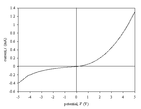
Figure 3.9.
Current-voltage characteristics for post-annealed oxidised diamond film with
one 3LM contact and one gold contact (sample B129a).
Figure 3.9 shows a current-voltage was measured using one 3LM contact and the other contact in the gold spot on oxidised terminated sample. A Shottky barrier was observed.
Resistance measurements are
shown in the next table:
|
Step of the
production |
Resistance (W) |
Sheet Resist. (Wcm) |
|
|
2 point probe |
4 point probe |
||
|
As grown |
- |
2569 |
5.83 |
|
After chromic acid reflux |
- |
22667 |
51.45 |
|
After annealing |
26620ª |
5670ª |
12.87 |
Table 3.2. Data from four point probes resistance measurements of the different stages in the production of the three layer metal contact.
Analysing data from above
table, resistance values for hydrogen and oxygen terminated samples for two 3LM
contacts are different. Hydrogen terminated material presents a higher
conductivity than the oxygen one 43-46. When the hydrogen conductive layer is removed from
the surface the resistance of the film increases 47-50. If the data for the annealing process is analysed
the two point probe has a bigger value than the four point probe and it is in a
ratio 3:1. Two point probe measures the resistance of the sheet material and
the contact resistance. Four point probe only measures the resistance of the
sheet between the contacts. Proportionality between four and two point probes
correspond approximately with the increase of the length between the contact
points when the experimental set-up is modified from 4 point probe to 2 point
probe. To explain the fact that the annealed sample is less resistance than the
oxidised one reconstruction of the structure in the surface, possible
graphitation or displacement of hydrogen from inner layers to the surface has
been suggested 2, 3, 17, 51-58.
Lack of accuracy was a
problem during the deposition of the different metals. The main source was the
vibration produced by the rotary pump in the evaporator chamber during the
metal depositions this caused a slight displacement in the mask creating a
faulty deposition and then a deficient contact.
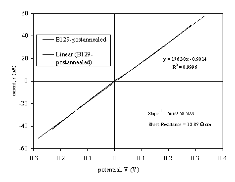
Figure 3.10. Four point probe current-voltage characteristics for post-annealed diamond film with two 3LM contacts (sample B129a).
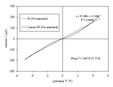
Figure 3.11.
Current-voltage characteristics for post-annealed diamond film with two 3LM
contacts (sample B129a).
Many steps of the production
of the contacts not only were long in terms of time but the probability of a
possible mistake was increased dramatically:
·
When
the annealing was not performed correctly, no TiC was formed giving a contact
very badly adhered on the surface sample. Frequently delamination was observed.
·
The
heating stage was a delicate step because it could produce a change of surface
diamond structure (appearance of graphite on the surface)
This 3LM electrical contact
was limited to oxidised diamond surface. Some modifications were done trying to
adapt the process to hydrogenated diamond surface. A PTFE cell (as described in
the electrochemical chapters) was used in order to restrict the area to which
hot chromic acid was applied to that of the contact.
The time consumed to produce
this type of contact was high. At least seven working days were required to
complete every single step in table 3.2. This was extended as access to sputter
apparatus and the high temperature furnace was restricted.
3.5.3. Conclusions
An Ohmic response has been found over a reduced applied potential range (-0.5 V to +0.5 V) for low doped boron polycrystalline diamond samples. However, further investigation will be required in order to improve the quality and reliability of this type of contact. Some investment will be necessary to achieve a high enough level of accuracy and purity to generate the 3LM contact under laboratory conditions. Due to all restrictions of this 3LM electrical contact, this technique was abandoned in favour of a new technique: titanium under layer contacts.
3.6. Titanium under layer contacts
Same ideas about the TiC
formation described in the 3LM electrical contacts were the starting point to
develop a new method (not described in the literature before) to form ohmic
contacts for low boron doped polycrystalline diamond.
A single strip of titanium
was deposited onto the surface of the silicon substrate before the diamond
deposition. Selective diamond growth on top of this metal layer was achieved by
leaving a smooth section of silicon which provided few nucleation sites. As the
diamond formed at raised temperatures, a metal carbide would form without the
need for a separate annealing step after the growth process and, since the film
was being grown in the absence of an oxygen containing species, no protective
metals were needed to prevent oxidation of the titanium.
A description of the
titanium under layer (TiUL) electrical contact fabrication is detailed in this
section. TiUL electrical contact is analysed using simple techniques such as
current-voltage (i-V) curves and four
point probe resistance measurements. The range of application of this contact
is given in terms of the doping level of the boron doped polycrystalline
diamond sample.
3.6.1. Construction
A silicon substrate was abraded
with diamond powder to create nucleation sites. The abrasion was not completed
in the whole silicon surface. One strip of the sample was left smooth in order
to suppress diamond growth on this region.
After removing the excess of
diamond powder using IPA soaked cotton sticks the sample was further cleaned in
an ultrasonic bath, only the abraded area was dipped in IPA solution. The
substrate was then dried at 100 ºC in a vacuum oven and stored in an evaporated
chamber. The silicon sample was covered with a mask such that a small fraction
of the abrasion zone and the whole of the non-abraded silicon was exposed. The
sample was heated under vacuum to remove any possible physisorbed species. In
the next step titanium was deposited (approximately between 100nm and 150 nm)
and then allowed to cool under vacuum to reach room temperature. The silicon
sample was then transferred to the CVD diamond chamber. During the growth of
the diamond film, an in situ
generation of titanium carbide was achieved with no risk of possible oxidation
due to the hydrogen atmosphere present in these conditions.
When the growth was over and
the diamond sample had reached room temperature under vacuum conditions, a wire
could be attached using silver paint and protected with an epoxy resin
adhesive. Table 3.3 is a summary of the production process for TiUL contacts.
Step
|
Description |
Step |
|
|
1 |
Nucleation
pre-treatment |
(a)
Abrade with diamond powder to provide nucleation sites, leaving a
strip of smooth silicon |
1.a |
|
2 |
Removing
diamond dust |
(a) Wipe with IPA soaked cotton sticks (b)
Place in a beaker of IPA in an ultrasonic bath, Leaving the non abraded
area out of the bath (c)
Rinse sample with IPA flowing away from smooth End |
2.a |
|
2.b |
|||
|
2.c |
|||
|
3 |
Titanium
deposition |
(a)
Load samples into evaporator (b)
Load metal into the basket (c)
Place mask over the sample, leaving the smooth area and small part of
the abraded area exposed (d)
Evacuate chamber (e)
Heat sample to remove physisorbed species (f)
Evaporate titanium onto diamond surface (g)
Reach room
temperature under vacuum
(h) Repeat from 2nd step until obtain desired thickness |
3.a |
|
3.b |
|||
|
3.c |
|||
|
3.d |
|||
|
3.e |
|||
|
3.f |
|||
|
3.g |
|||
|
3.h |
|||
|
4 |
Diamond
growth |
(a)
Load substrate into chamber (b)
Evacuate chamber (c)
Pre-heat substrate (d)
Deposit diamond for several hours (e)
Initially cool in hydrogen atmosphere (f)
Reach room temperature under vacuum |
4.a |
|
4.b |
|||
|
4.c |
|||
|
4.d |
|||
|
4.e |
|||
|
4.f |
|||
|
5 |
Attachment
of wires |
(a)
Attach copper wire with silver paint (allow to dry) (b)
Cover silver paint with epoxy resin for protection |
5.a |
|
5.b |
|||
Table 3.3. Summary of the production process for TiUL contacts
A schematic diagram of the
titanium under layer contact is shown in figure 3.12 and figure 3.13
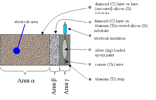
Figure 3.12. Plane
schematic view of titanium under layer contact (not to scale). Area a is a region of diamond growth on abraded silicon.
Area b is a region of diamond
growth on titanium coated silicon. Area g is a region of a titanium coated silicon with no
diamond present (silicon was not abraded)
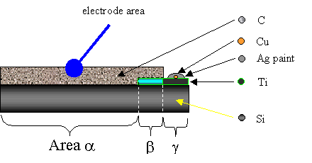
Figure 3.13. Perspective schematic view of titanium under layer contact (not to scale). Area a is a region of diamond growth on abraded silicon. Area b is a region of diamond growth on titanium coated silicon. Area g is a region of a titanium coated silicon with no diamond present (silicon was not abraded).
As explained in figures 3.12
and 3.13 the standard procedure to fabricate a titanium under layer contact was
the deposition of a single strip of metal on the silicon substrate. This
procedure was employed for electrochemical measurements in order to maximise
the sample area. However, it was not adequate for the electrical
characterisation. A double strip diamond sample (see figures 3.14 and 3.15)
(B147a) was fabricated to properly characterise the electrical contact.

Figure 3.14. Plane schematic view of double strip under layer titanium contact (not scale). Area a is a region of titanium coated silicon with no diamond present (silicon was not abraded). Area b is a region of diamond growth on titanium coated silicon. Area c is a region of diamond growth on abraded silicon
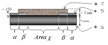
Figure 3.15.
Perspective schematic view of double strip under layer titanium contact (not
scale). Area a
is a region of titanium coated silicon with no diamond present (silicon was not
abraded). Area b
is a region of diamond growth on titanium coated silicon. Area c is a
region of diamond growth on abraded silicon.
A series of structural
characterisation experiments were performed on the titanium under layer double
contacts using SEM and optical microscopy techniques.
The SEM equipment and the
conditions to work with the diamond samples were described in section 2.2.10. A
Zeiss Axiolab Optical Microscope fitted with Zeiss Epiplan lenses was
frequently used to view the samples. Objective lenses of 5 ´, 10 ´, 50 ´ and 100 ´ coupled with an 10 ´ eyepiece to give a range of magnifications
from fifty to one thousand.
Images were captured with a
JVC TK-1280E Colour Camera attached to an Olympus BH2 Optical Microscope fitted
with a 10 ´ eyepiece and 4 ´, 10 ´, 20 ´ and 50 ´ objective lenses.
The images shown below refer
to the double contact sample, the regions are indicated on figures 3.14 and
3.15.
Figures 3.16 to 3.18 show a
randomly oriented diamond film on area c. If the images are analysed
in more detail no pinholes or cracks are presented. However diamond grit from
the preparation of the substrate to grow diamond is found in the images
(figures 3.16 and 3.18).
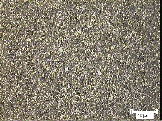
Figure 3.16. Optical microscopy image of the central section (area c) taken with a 50 ´ objective lens (sample B147a).
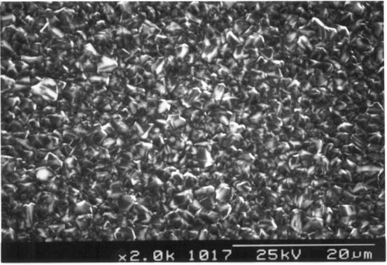
Figure 3.17. Randomly oriented diamond film in central section (area c) (sample B147a).
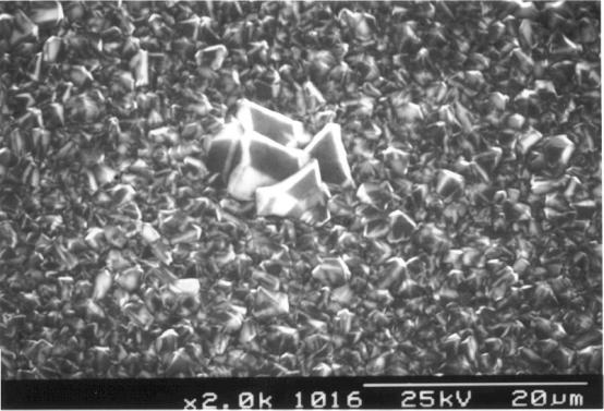
Figure 3.18. Randomly oriented diamonds with an inclusion of diamond grit. SEM image was taken in central section (area c) (sample B147a).
The boundaries between the
different growth areas are shown in figures 3.19 to 3.25.
Figures 3.19 to 3.22 show
the boundary between areas a and b. Areas are quite well defined. Low diamond
coverage can be seen in the titanium non-abraded zone and good coverage for the
abraded part. SEM images compliment the optical images with more details.
Figures 3.23 to 3.25 show
the boundary between areas b and c. The change in brightness allows identification
of each zone in the optical images.

Figure 3.19. Optical microscopy image of the boundary between areas a and b taken with a 20 ´ objective lens (sample B147a).
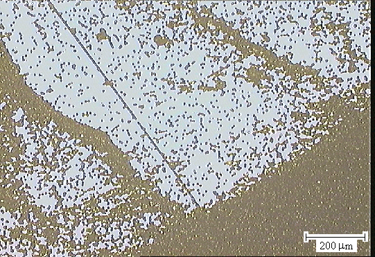
Figure 3.20. Optical
microscopy image of the boundary between areas a and b
taken with a 10 ´
objective lens (sample B147a).
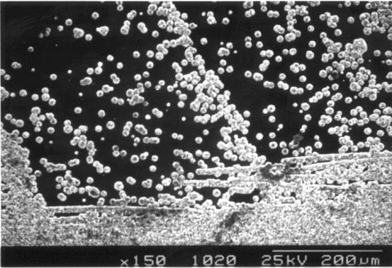
Figure 3.21. SEM image of the boundary between areas a and b (sample B147a).
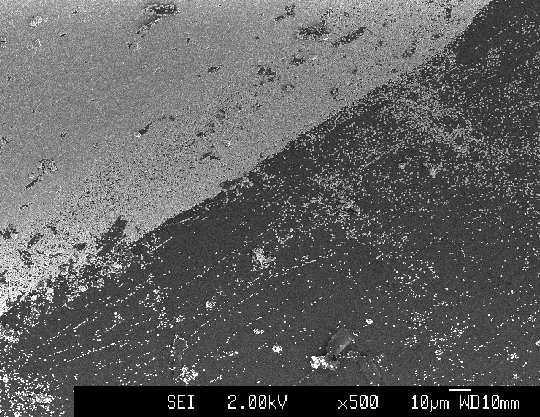
Figure 3.22. SEM image of the boundary between areas a and b (sample B147a).
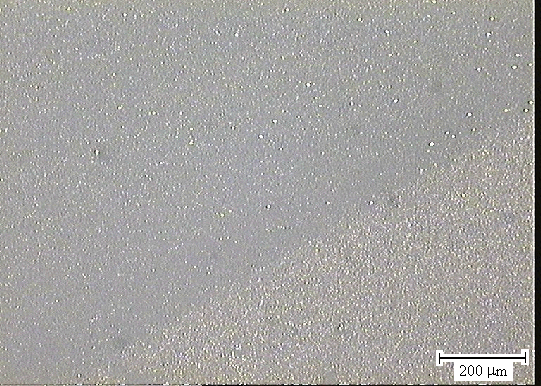
Figure 3.23. Optical microscopy image of the boundary between areas b and c taken with a 10 ´ objective lens (sample B147a).
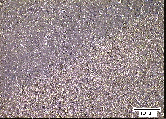
Figure 3.24. Optical
microscopy image of the boundary between areas b and c
taken with a 20 ´
objective lens (sample B147a).
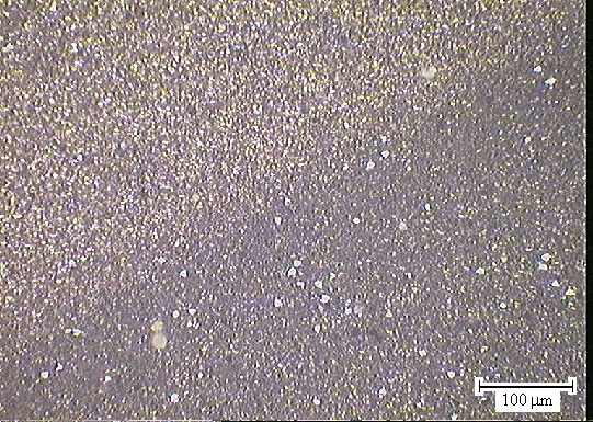
Figure 3.25. Optical
microscopy image of the boundary between areas b and c
taken with a 20 ´
objective lens (sample B147a).
3.6.2. Results and discussion
Current-voltage (i-V) curves were employed to describe
the quality of the contacts using a Solartron 1287 Electrochemical Interface
potentiostat in two-electrode mode. The scan rate was 50 mV/s.
A series of four point probe
measurements were taken to obtain values for the sheet resistance of the samples
without measuring the contact resistance (see section 3.5.2 for more details).
Figure 3.26 shows the
current voltage plot for a low doped (50 pppm) diamond sample with two TiUL
contacts (sample b147). The plot is linear over a potential range of approximately
ten volts (see insets).
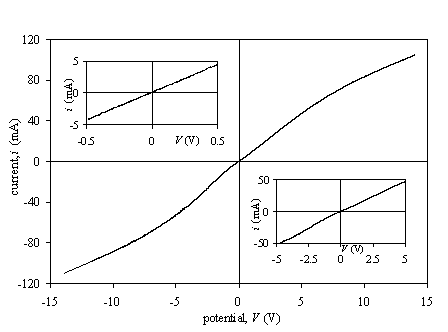
Figure 3.26.
Current-voltage characteristics for an as-grown diamond film with two TiUL
contacts (sample B147a)
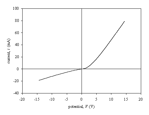
Figure 3.27.
Current-voltage characteristics for an oxidised diamond film with one TiUL
contact and one gold contact (sample B147a).
Figure 3.27 shows a
current-voltage was measured using one TiUL contact and the other contact is a
gold spot that was deposited after the oxidation of the diamond surface. A
Shottky barrier was observed as suggested in the literature for low doped
diamond/gold barriers 16-20.
Comparing the TiUL contact
fabrication process against the 3ML one, following advantages are noted:
·
There
was a drastic reduction in the average time necessarily to generate the contact
on the sample. The whole process could be completed in three working days.
·
The
number of steps was reduced thus decreasing the probability of contact failure.
·
Titanium
carbide layer was synthesised at the same time that the diamond film was
growing. In such conditions no oxidation was possible for the titanium strip
giving durability, strength and a long life to the contact.
·
As
this contact is underneath the diamond film, more diamond surface was available
to perform electrochemical experiments.
The only disadvantage was
that post-treatments were limited for the titanium under layer contact. It was
not possible to apply a reflux in a chromic acid bath. Only by protecting very
carefully the contact with PTFE adhesive film could the samples to be dipped in
hot chromic acid. An alternative was the selective oxidation of a determinate
zone using a PTFE cells (as presented and explained in chapter 5).
3.6.3. Conclusions
Ohmic response has been found over a wide applied potential range (-5 V to +5 V) for low doped boron polycrystalline diamond samples. This range is over the limits of the electrochemical potentials applied in this study
Easy fabrication process, good reproducibility and long life contact suggests TiUL electrical contacts as the ones to be used in boron low doped polycrystalline diamond electrochemical studies.
3.7. Summary
Highly doped diamond films
do not need any special electrical connection to obtain Ohmic contacts. However
low doped diamond requires the carbide formation in the electrical contact to
obtain the Ohmic properties. Different methods have been presented to reach it.
Titanium underlayer contacts appears to be the quickest in the fabrication
stage and most reliable of the electrical contacts studied.
3.8. References
1 S. M. Sze, 'Semiconductor
devices, physics and technology', ed. J. Wiley, 1985.
2 K. L. Moazed, R. Nguyen, and
J. R. Zeidler, IEEE Electron Device Lett.,
1988, 9, 350.
3 K. Moazed, L., J. R.
Zeidler, and M. Taylor, J., J. Appl.
Phys., 1990, 68, 2246.
4 S. Alehashem, F. Chambers,
J. W. Strojek, G. M. Swain, and R. Ramesham, Anal. Chem., 1995, 67,
2812.
5 C. H. Goeting, J. S. Foord,
F. Marken, and R. G. Compton, Diam.
Relat. Mater., 1999, 8, 824.
6 T. N. Rao, I. Yagi, T. Miwa,
D. A. Tryk, and A. Fujishima, Anal. Chem.,
1999, 71, 2506.
7 B. V. Sarada, T. N. Rao, D.
A. Tryk, and A. Fujishima, J.
Electrochem. Soc., 1999, 146,
1469.
8 M. Yanagisawa, L. Jiang, D.
A. Tryk, K. Hashimoto, and A. Fujishima, Diam.
Relat. Mater., 1999, 8, 2059.
9 F. J. Del Campo, C. H.
Goeting, D. Morris, J. S. Foord, A. Neudeck, R. G. Compton, and F. Marken, Electrochem. Solid State Lett., 2000, 3, 224.
10 S. Ferro, A. De Battisti, I.
Duo, C. Comninellis, W. Haenni, and A. Perret, J. Electrochem. Soc., 2000, 147,
2614.
11 B. V. Sarada, T. N. Rao, D.
A. Tryk, and A. Fujishima, Anal. Chem.,
2000, 72, 1632.
12 A. J. Saterlay, S. J.
Wilkins, C. H. Goeting, J. S. Foord, R. G. Compton, and F. Marken, J. Solid State Electrochem., 2000, 4, 383.
13 A. J. Saterlay, F. Marken,
J. S. Foord, and R. G. Compton, Talanta,
2000, 53, 403.
14 Y. Einaga, G. S. Kim, S. G.
Park, and A. Fujishima, Diam. Relat.
Mater., 2001, 10, 306.
15 A. J. Saterlay, S. J.
Wilkins, K. B. Holt, J. S. Foord, R. G. Compton, and F. Marken, J. Electrochem. Soc., 2001, 148, E66.
16 G. H. Glover, Solid State Electron., 1973, 16, 973.
17 H. Shiomi, H. Nakahata, T.
Imai, Y. Nishibayashi, and N. Fujimori, Jap.
J. App. Phys., 1989, 28, 758.
18 S. A. Grot, G. S.
Gildenblat, C. W. Hatfield, A. R. Badzian, and T. Badzian, IEEE Electron Device Lett., 1990, 11, 371.
19 S. A. Grot, G. S.
Gildenblat, C. W. Hatfield, C. R. Wronski, A. R. Badzian, T. Badzian, and R.
Messier, IEEE Electron Device Lett.,
1990, 11, 100.
20 S. A. Grot, C. W. Hartfield,
G. S. Gildenblat, A. R. Badzian, and T. Badzian, App. Phys. Lett., 1991, 58,
1542.
21 A. T. Collins, E. C.
Lightowlers, and A. W. S. Williams, Suppl.
Indust. Diam. Rev., 1970, 30,
19.
22 R. Tenne, K. Patel, K.
Hashimoto, and A. Fujishima, J.
Electroanal. Chem., 1993, 347,
409.
23 C. Reuben, E. Galun, H.
Cohen, R. Tenne, R. Kalish, Y. Muraki, K. Hashimoto, A. Fujishima, J. E.
Butler, and C. Levy-Clement, J.
Electroanal. Chem., 1995, 396,
233.
24 B. Ohtani, Y. H. Kim, T.
Yano, K. Hashimoto, A. Fujishima, and K. Uosaki, Chemistry Letters, 1998, 953.
25 Z. Y. Wu, T. Yano, D. A.
Tryk, K. Hashimoto, and A. Fujishima, Chem.
Lett., 1998, 503.
26 T. Yano, D. A. Tryk, K.
Hashimoto, and A. Fujishima, J.
Electrochem. Soc., 1998, 145,
1870.
27 A. Manivannan, D. A. Tryk,
Fujishima, and A., Electrochem. and
Solid-State Lett., 1999, 2, 455.
28 S. Nakabayashi, D. A. Tryk,
A. Fujishima, and N. Ohta, Chem. Phys.
Lett., 1999, 300, 409.
29 S. Nakabayashi, N. Ohta, and
A. Fujishima, PCCP, 1999, 1, 3993.
30 H. Notsu, I. Yagi, T. Tatsuma,
D. A. Tryk, and A. Fujishima, Electrochem.
Solid State Lett., 1999, 2, 522.
31 E. Popa, H. Notsu, T. Miwa,
D. A. Tryk, and A. Fujishima, Electrochem.
Solid State Lett., 1999, 2, 49.
32 T. N. Rao, D. A. Tryk, K.
Hashimoto, and A. Fujishima, J.
Electrochem. Soc., 1999, 146,
680.
33 I. Yagi, K. Tsunozaki, D. A.
Tryk, and A. Fujishima, Electrochem. and
Solid-State Lett., 1999, 2, 457.
34 I. Yagi, H. Notsu, T. Kondo,
D. A. Tryk, and A. Fujishima, J.
Electroanal. Chem., 1999, 473,
173.
35 T. Yano, E. Popa, D. A.
Tryk, K. Hashimoto, and A. Fujishima, J.
Electrochem. Soc., 1999, 146,
1081.
36 S. Yoshihara, K. Shinozaki,
T. Shirakashi, K. Hashimoto, D. A. Tryk, and A. Fujishima, Electrochim. Acta, 1999, 44,
2711.
37 T. Tachibana, B. Williams,
E., and J. Glass, T., Phys. Rev. B,
1992, 45, 11968.
38 H. J. Looi, L. Y. S. Pang,
M. D. Whitfield, J. S. Foord, and R. B. Jackman, Diam. Relat. Mater., 2000, 9,
975.
39 L. J. Brillson, J. Vac. Sci. Tech., 1982, 20, 652.
40 L. J. Brillson, Surf. Sci. Rep., 1982, 2, 123.
41 H. Shiomi, Y. Nishibayashi,
N. Fujimori, and K. Kobashi, Japan J.
Appl. Phys., 1991, 30, 1363.
42 D. R. Linde, in 'CRC
Handbook of Chemistry and Physics', ed. D. R. Linde, 1994.
43 F. Maier, M. Riedel, B.
Mantel, J. Ristein, and L. Ley, Phys.
Rev. Lett., 2000, 85, 3472.
44 J. Ristein, F. Maier, M.
Riedel, J. B. Cui, and L. Ley, Physica
Status Solidi a-Applied Research, 2000, 181, 65.
45 A. Bergmaier, G. Dollinger,
A. Aleksov, P. Gluche, and E. Kohn, Surf.
Sci., 2001, 481, L433.
46 H. J. Looi, L. Y. S. Pang,
A. B. Molloy, F. Jones, J. S. Foord, and R. B. Jackman, Diam. Relat. Mater., 1998, 7,
550.
47 J. Shirafuji and T. Sugino, Diam. Relat. Mater., 1996, 5, 706.
48 T. Sugino, Y. Iwasaki, S.
Kawasaki, R. Hattori, and J. Shirafuji, Diam.
Relat. Mater., 1997, 6, 889.
49 T. Sugino, Y. Iwasaki, S.
Kawasaki, Y. Yuuko, R. Hattori, and J. Shirafuji, Diam. Relat. Mater., 1998, 7,
677.
50 P. Gonon, S. Prawer, D. N.
Jamieson, and K. W. Nugent, Diam. Relat.
Mater., 1997, 6, 314.
51 C. Jany, F. Foulon, P.
Bergonzo, and R. D. Marshall, Diam.
Relat. Mater., 1998, 7, 951.
52 H. J. Looi, R. B. Jackman,
and J. S. Foord, Appl. Phys. Lett.,
1998, 72, 353.
53 M. Werner, R. Job, A.
Denisenko, A. Zaitsev, W. R. Fahrner, C. Johnston, P. R. Chalker, and I. M.
BuckleyGolder, Diam. Relat. Mater.,
1996, 5, 723.
54 H. Kiyota and E. Matsushima,
Appl. Phys. Lett., 1995, 67, 3596.
55 C.F. Chen and S. Chen, Diam. Relat. Mater., 1995, 4, 451.
56 M. Werner and O. Dorsch, Diam. Relat. Mater., 1994, 3, 983.
57 J. Vanderweide and R. J.
Nemanich, Phys. Rev. B, 1994, 49, 13629.
58 T. Tachibana, B. Williams,
E., and J. Glass, T., Phys. Rev. B,
1992, 45, 11975.