Chapter 5
Electrochemical studies of moderately boron doped diamond in non
aqueous electrolyte
5.1. Introduction
Studies of diamond
electrodes in non aqueous solvents are very limited. It has been reported that
diamond electrodes in non aqueous electrolyte posses an increased potential,
allowing a fifth peak for the reduction of C60 to be observed 1. In addition diamond electrodes have been employed in
the generation of solvated electrons in ammonia 2. Both studies were performed using highly boron doped
diamond. In this chapter, electrochemical studies of moderately boron doped
diamond in non-aqueous solvents are presented. A proper investigation requires
locating the band edges in the chosen medium. The determination of the band
edges is performed by Mott-Shottky studies. These allow the calculation of the
flat band potential and therefore the band edges. As diamond electrodes are
under influence of their surface termination separate Mott-Shottky studies are
required with hydrogen and oxygen terminated diamond electrodes. Additional
cyclic voltammetric studies are presented for both types of surface
termination. Mott-Shottky data and
cyclic voltammograms are compared and explained in terms of the band edge
localisation and the theory developed in the chapter 4.
5.2. Potential distribution across the semiconductor-electrolyte
interface
Consider initially a p-type
semiconductor in equilibrium with a redox couple. Equilibrium is reached when
the Fermi level of the semiconductor is equal to the Fermi energy associated
with the redox couple (see figure 5.1)
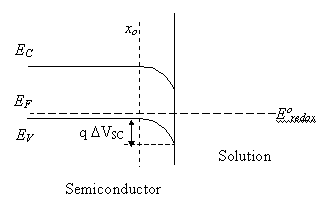
Figure 5.1. Energy diagram of the semiconductor-electrolyte interface under equilibrium. The Fermi level energy (EF) is equal to the redox potential energy (Eºredox).
The depletion layer, more
commonly known as space charge region, produces a bending of the bands to lower
energies.
Under potentiostatic control
the applied potential is established between the working electrode and the reference
electrode. If the interface is considered as ideally polarizable (electrons
cannot be exchanged with the electrolyte), the zero of potential is that at
which the potential in the bulk semiconductor matches that of redox couple ate
the reference electrode, see figure 5.2.
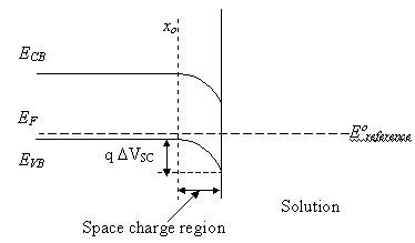
Figure 5.2. Energy diagram of an ideally polarisable interface at zero potential. The Fermi level energy (EF) is equal to the reference electrode energy (Eºreference).
From figure 5.2 it is
apparent that the concentration of the electrons in the space charge region
depends on the potential difference between the working electrode
(semiconductor) and the reference. At this point it is necessary to consider
the other side of the working electrode/ electrolyte junction, the Helmholtz
double layer. Briefly, when the supporting electrolyte is in high
concentration, this region contains the nonadsorbed ions that represent the
counter charge. The thickness of this layer is smaller than the space charge
region (see figure 5.3).

Figure 5.3. Schematic representation of the potential
drop (a) and charge across the semiconductor electrolyte interface under
depletion conditions.
In figure 5.3.a the
potential distribution across the interface is shown taking the potential of
the bulk of the solution as zero. The potential drop across the space charge
region (DVSC) occurs over
a larger distance than the potential drop across the Helmholtz layer (DVH), this is because DVSC results from ionisation of the
acceptors in the solid, whilst DVH is due to the
ions accumulated a few angstroms away from the surface (see figure 5.3b).
Since the charge in both
regions is equal but with opposite sign, the capacitance of the space charge
region is normally negligible in comparison to the Helmholtz capacitance. Under
these conditions, DVH is constant
and any possible change in the applied potential between working and reference
electrode will appear in DVSC. Thus the
potential in the bulk of the working electrodes (E) is given by:
![]() [equation 5.1]
[equation 5.1]
where Vfb is
the flat band potential. At this potential, the surface concentration of holes
is equal to the bulk. At more positive potentials than the Vfb, the surface concentration of electrons is decreased
creating an accumulation layer of majority carriers and the bending of the
bands at the surface to higher energies. At potentials more negative than the Vfb, electrons produce a
depletion layer, bending downwards at the surface to lower energies (see figure
5.4).
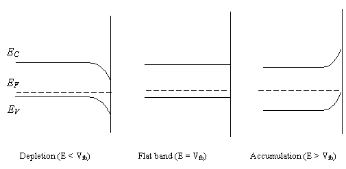
Figure
5.4. Potential dependence of the band bending for a p-type semiconductor. NSC : free
carrier concentration
Under depletion conditions,
charging comes from the electron affinity of the acceptors. If the density of
the charge is assumed constant in the space charge region, Poisson’s equation
can be written as
![]()
[equation 5.2]
After integrating twice and
assuming that the electric field (dV/dx)
is zero at xo, a long way
from the surface and that V is zero
in the bulk of the semiconductor, the Shottky relation can be obtained
![]()
[equation
5.3]
where w is the width of the space charge region.
Considering Gauss’s law:
![]()
[equation
5.4]
where A is the surface area
of the electrode. Substituting the integrated Poisson’s equation into equation
5.4, the capacitance of the space charge region (CSC) is
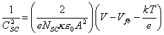
[equation
5.5]
The above equation is known
as Mott-Schottky relationship. From equation 5.5, CSC-2
is linearly dependent on V, with the slope inversely proportional to NSC
and related to Vfb.
The flatband potential is important in determining the conduction or the valence band edges for a semiconductor on the vacuum reference scale of energies. Once Vfb is known, EVB and ECB can be calculated from the relations
![]()
(p-type
semiconductor) [equation 5.6]
![]()
(n-type semiconductor) [equation 5.7]
where EVB and ECB
are the band edges of the valence band and the conduction band; NVB and NCB, are the effective density of states in the valence
and conduction bands respectively for a p- and n-type semiconductors, data
obtained from solid state measurements. Once ECB or EVB
is determined the other can be easily found provided Eg is known.
5.3. Experimental set-up
Electrochemical experiments were performed using a three electrode
system. This section descibes the apparatus used.
5.3.1. Electrolyte
solutions
Anhydrous acetronitrile (99.9% pure) was used as solvent and 0.1 mol
dm-3 tetrabutylammonium perchorate (TBAP) as supporting electrolyte.
Two different solutions were prepared contaning 1´10-3 mol dm-3 of either ferrocene (FeCp2)
or bis(pentamethylcyclopentadienyl) iron (FeCp2*).
Glassware was cleaned with a five step process:
1.
soaking in a chromic acid bath (saturated
potasium dichromate (K2Cr2O7) in concentrated
sulfuric acid (H2SO4).
2.
immersing and rinsing in deionised water
(18.3 MW cm ultrapure deionised
water (Millipore)).
3.
soaking in an aqua regia bath (1:3 nitric
acid (HNO3)/ hydrochloric acid
(HCl)).
4.
inmmersing and rising in deionised water.
5.
placing in an oven at 100ºC for 30 minutes
and checking no moisture remained.
After this routine all the glassware was kept in the dry box under
argon atmosphere.
All the solutions were prepared under dry box conditions to ensure
that no moisture or oxygen entered the solutions. To double check that no
residual oxygen was present in the solutions they were purged with standard
laboratoy grade oxygen-free argon (Ar) for aproximmately 10 minutes inside the
dry box before any electrochemical experiment was done.
5.3.2 Electrochemical Cells
The main type of cell used
in these studies was a single chamber design. A schematic diagram is shown in
figure 5.5. This cell design proved ideal for performing electrochemistry with
silver paint, three layer metal and titanium underlayer contacts.
The electrochemical cells
were fabricated from white cylinders of PTFE †
(50 mm in diameter). A central bore was removed from the main segment of
the cell to provide a reservoir for the electrolyte. The diamond sample that
was to be used as a working electrode (WE) was laid horizontally and sandwiched
between two PTFE cylinders. A 4mm hole in the base of the main piece and an ‘O’
ring (3.5 mm internal diameter) exposed a selected area of the electrode
surface to the electrolyte. Therefore, the approximate electrode area exposed
to the electrolyte was 0.4 cm2 (40 mm2).

Figure 5.5. A schematic diagram of an electrochemistry cell
The base of the cell was
tapered to allow small samples to be used. All samples had to be flat and the
minimum sample size was 1 cm ´ 1 cm. Typical sample
dimensions were 1.5 cm ´ 1 cm.
The bottom piece of PTFE was
attached to a brass plate to provide a stable base.
A transparent top piece was
fitted over the cell. The reference electrode (RE) and the counter electrode
(CE) were placed through holes in the top. They were held in place by rubber
rings (not illustrated in figure 5.5). Two additional holes allowed for
deoxygenating to be performed. Argon could be bubbled through the electrolyte via
a needle that was passed down into the solution.
Control experiments could be
performed with platinum (Pt) working electrodes. Platinum wires could be passed
down through one of the gas inlets.
5.3.3. Counter Electrodes
Platinum (Pt) counter
electrodes were made from a curled square of platinum mesh attached to a
platinum wire. This provided a suitably large surface area. A glass tube was
used to hold the electrode. This was designed with the same diameter as the
reference electrode. The tube was sealed to the platinum wire at the bottom of
the electrode. The top of the tube, which was never submersed into the
electrolyte, was sealed with epoxy resin. Nickel wire was used inside the glass
tube because it was less expensive than the platinum wire. The wire was wound
round a notch at the top of the electrode, so that the weight of the attached
crocodile clip did not apply a force on to the platinum-nickel join or the
platinum-glass seal. A quick fit stopper was fitted to the top of the electrode
to provide compatability with a number of other designs of electrochemical
cell. A diagram of a counter electrode is shown in figure 5.6.
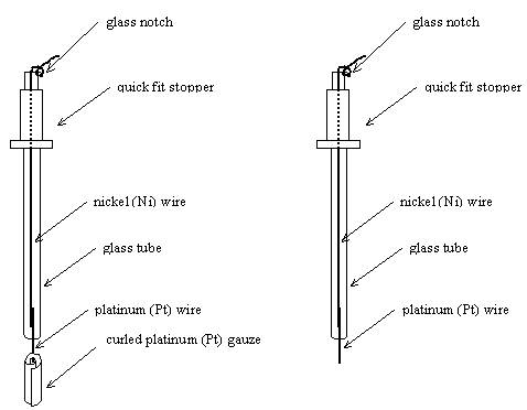
Figure 5.6. In the left side, a schematic diagram of a platinum counter electrode. In the right side, a schematic diagram of a platinum wire electrode.
5.3.4. Reference Electrodes
Ferrocene | Ferrocenium
cation (FeCp2|FeCp2+) reference electrodes
were used. These electrodes were made from a glass frit and a platinum wire
electrode. The glass frit was filled with a solution containing 1´10-3 mol dm-3 of
ferrocene/ferrocenium in 0.1 mol dm-3 of TBAP/CH3CN (see
figure 5.7). To avoid any possible evaporation process the top of the reference
electrode (where the glass frit and the platinum counter electrode join) was
sealed with PTFE tape.
The formal potentials, Eº¢, are given in this chapter vs ferrocene |
ferrocenium couple, as recommended by IUPAC 3 when the electrolyte is not aqueous. The formal
potential for FeCp2 | FeCp2+ is 0.38 V
relative to the aqueous satured calomel electrode (SCE) at 298 K 4.
Experimental measurements
were done to check the relationship of the ferrocene couple and SCE. Neglegible
differences were observed between the experimental and the literature data.
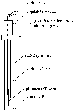
Figure 5.7. A schematic diagram of a ferrocene reference electrode.
5.3.5 Potentiostats
Cyclic voltammometric
measurements were performed using an EG&G 273 Princeton Applied Research
instrument that was controlled using Research Electrochemistry software.
Impedance measurements were performed using a Solartron 1286 potentiostat and a Solartron 1250 Frequency Response Analyser (FRA). The instruments were controlled using Z-plot software. In all ac experiments a modulation amplitude of 10 mV was applied.
5.3.6. The dry box
A standard dry box was
modified on one side to install one parallel and three BNC electrical
connections. This modification allowed control of the electrochemical
experiments through a computer. The dry box operates in a simple way. It is
continuously filled by argon gas (standard laboratoy grade oxygen-free argon
gas cylinder (BOC)). During that process as
oxygen is lighter than argon oxygen will be removed through the exhaust lines.
The argon gas is dried when it passes thorough a column filled with dry sieves.
A pump is used to recirculate the argon gas. An air-lock is employed to allow
materials to be put in and out material without introducing moisture or oxygen
to the dry box. Neoprene gloves are used to operate inside the dry box (see
figure 5.8).
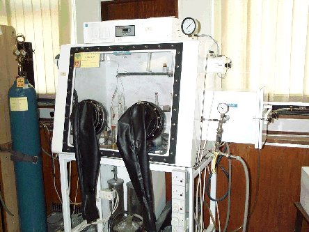
Figure 5.8. A picture of the dry box
All electrochemical
experiments were performed in the dry box in such conditions that the amount of
water vapour was less than 6 ppm by volume.
5.4. Mott-Schottky Plots
To establish the position of
the band edges of p-type diamond in acetonitrile Mott-Schottky analyses were
undertaken.
Plots 1/(capacitance)2
against applied potential, recorded at different frequencies, for both
hydrogenated and oxygenated boron doped diamond electrodes immersed in
acetronitrile containing 0.1 mol dm-3
TBAP are displayed in figure 5.9 and figure 5.10.
Although Mott-Schottky
theory suggests that plots should be independent of the measuring frequency
(see section 5.2) this behaviour is rarely observed for semiconductor
electrodes.
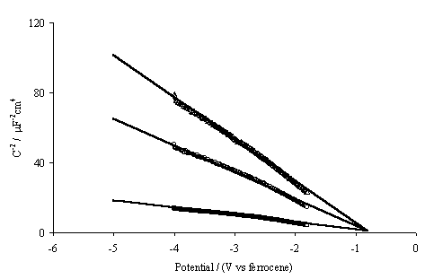
Figure 5.9. Mott-Schottky plots for semiconducting hydrogen terminated boron doped diamond electrode. Three frequencies of modulation were recorded; D 10 KHz, O 5 KHz and ÿ 1 KHz. Linear extrapolation of the experimental data has a common intercept approximately –0.8 V. Potential relative to the ferrocene standard couple.

Figure 5.10. Mott-Schottky plots for semiconducting oxygen terminated boron doped diamond electrode. Three frequencies of modulation were recorded; à 20 KHz, O 10 KHz and [] 5 KHz. Linear extrapolation of the experimental data has a common intercept approximately 1.5 V. Potential relative to the ferrocene standard couple.
Surface roughness,
dielectric relaxation and the influence of surface states have been advanced as
explanations of the frequency dispersion in Mott-Schottky plots5.
In order to calculate the
free carrier concentration equation 5.5 at 298 K (NSC in cm-3,V in V, CSC
in mFcm-2) can be simplified to:
[equation
5.8]
where diamond e = 5.5.
Using the data recorded at a
frequency of 10 KHz a free carrier concentration (NSC) of 1.1´1018 cm-3 was determined for both the hydrogenated
and oxygenated samples. This figure compares favourably with the experimental
conditions employed during film preparation; a boron to carbon ratio of 50 ppm
in the gas phase suggest a boron density of 5.7´1018 cm-3
in the crystal, assuming the boron concentration in the solid is directly
proportional to that in the gas phase.
At the hydrogenated surface
the Mott-Schottky plots are linear between –1.8 V and –4.0 V and posses a
common intercept. The plots indicate that the valence band edge (using equation
5.6), relative to the ferrocene couple, lies at –0.8V. Given that the bandgap
of diamond is 5.4 eV this places the conduction band edge at –6.2 V on the same
scale, or at +1.3 eV relative to an electron in a vacuum 6. The fact that hydrogen terminated diamond has
negative electron affinity is one of the key reasons why this material is being
considered in field emission devices 7-23.
The change in surface bond
polarisation at the oxygen terminated surface relative to the hydrogenated
surface results in a large shift in the band edges 24. This is evident in the Mott-Schottky data for the
oxygenated p-type diamond electrode. In the case of the oxygenated diamond
surface a linear region is observed between 0.3V and –2.0 V; as for the
hydrogen terminated surface frequency dispersion is evident but a common
intercept is attained.
Analysis of the data
indicates that for oxygen terminated p-type diamond electrode in acetonitrile
the valence band edge lies at 1.5 V and the conduction band edge at –3.9 V 25, indicating positive electron affinity.
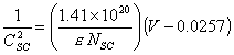
In figure 5.7 the energy
levels for the oxygen and hydrogen terminated surfaces of p-type diamond, as
determined from Mott-Schottky data, are shown. In addition the energy levels of
some common non-aqueous outer sphere redox couples are displayed 4, 26. To facilitate discussion the electron affinity of
graphitic carbon is also plotted, this energy level is a guide to energy of
graphitic surface states at the diamond/electrolyte interface 6. Elemental boron surface states are approximately
placed in the energy diagram 27,
28.
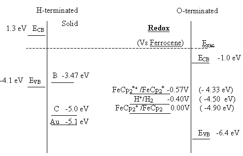
Figure 5.11. Proposed energy diagram for the diamond-electrolyte interface for hydrogen and oxygen terminated samples. H+/H2 = -0.4 V, FeCp2+ /FeCp2 0.00V ( -4.90 eV)
5.5. Cyclic voltammograms
In the figures 5.12 and 5.13
cyclic voltammograms for a platinum working electrode in 1´10-3 mol dm-3 FeCp2
and 1´10-3 mol dm-3 FeCp2*
in 0.1 M TBAP/MeCN respectively are displayed.
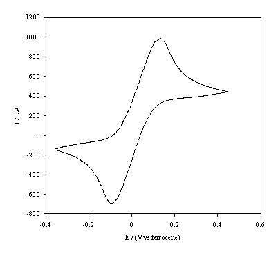
Figure 5.12. Cyclic
voltammetric i-E curve recorded at a
scan rate of 0.1 V s-1, of platinum working electrode in 1´10-3 mol dm-3 FeCp2.
Figure 5.13. Cyclic
voltammetric i-E curve recorded at a
scan rate of 0.1 V s-1, of platinum working electrode in 1´10-3 mol dm-3 FeCp2*.
In the figures 5.14, 5.15,
5.16, 5.17 cyclic voltammograms for hydrogen and oxygen surface terminated
diamond in both 1´10-3 mol dm-3
FeCp2 and 1´10-3 mol dm-3
FeCp2* in 0.1 M TBAP/MeCN are displayed.
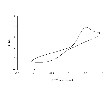
Figure 5.14. Cyclic voltammetric i-E curve recorded at a scan rate of 0.1 V s-1, of boron doped diamond electrode. A hydrogen terminated sample immersed in 1´10-3 mol dm-3 FeCp2.
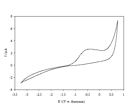
Figure 5.15. Cyclic voltammetric i-E curve recorded at a scan rate of 0.1 V s-1, of boron doped diamond electrode. A hydrogen terminated sample immersed in 1´10-3 mol dm-3 FeCp2*.
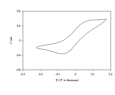
Figure 5.16. Cyclic voltammetric i-E curve recorded at a scan rate of 0.1 V s-1, of boron doped diamond electrode. An oxygen terminated sample immersed in 1´10-3 mol dm-3 FeCp2.
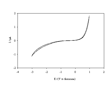
Figure 5.17. Cyclic voltammetric i-E curve recorded at a scan rate of 0.1 V s-1, of boron doped diamond electrode. An oxygen terminated sample immersed in 1´10-3 mol dm-3 FeCp2*.
At the hydrogen terminated surface, figure 5.14, well defined oxidation and reduction peaks are observed for the FeCp2+ / FeCp2 redox couple. The cathodic peak is distorted and the peak separation is approximately 1.2 V; it should be noted that the material was highly resistive and no iR compensation was employed when recording the voltammograms, and the kinetics of the redox couple appears to be slow. In contrast figure 5.15 shows that the oxidation of FeCp2* at the same surface is irreversible with negligible cathodic currents until voltages less than ‑2.5 V are achieved. This behaviour is explained in terms of the classical Marcus-Gerischer mechanism of electron transfer 6, 29-31. Reference to figure 5.11 indicates that the redox level of the FeCp2+ / FeCp2 couple lies within the valence band of the hydrogen terminated p-type diamond. Hence at the redox potential of the couple the Fermi level lies within a semiconductor band and reversible electrochemistry is observed. In comparison the redox level of the FeCp2*+ / FeCp2* couple lies almost at the band edge of the hydrogen terminated p-type diamond. Therefore, an anodic current flows only at potentials under which holes accumulate at the electrode surface whilst a small constant cathodic current flows due to the negligible overlap between the energy levels of the oxidised states and the valence band edge. At high negative overpotentials an increased cathodic current may be observed due to breakdown of the Schottky barrier. In summary the results indicate that the hydrogen terminated material is acting as a p-type semiconductor electrode when used in non-aqueous solvents.
The large shift in the band
edges with change in surface termination of p-type diamond results in the
cyclic voltammograms recorded at the oxygen terminated surface being markedly
different to those of the hydrogen terminated surface. The cyclic voltammogram
in figure 5.16 indicates that for the FeCp2+ / FeCp2
couple anodic and cathodic currents are observed at the oxygenated surface. The
current magnitude is considerably less than that for the hydrogenated surface
despite identical experimental parameters. In figure 5.17 the cyclic
voltammogram for the FeCp2*+ / FeCp2*
couple is displayed, it is apparent that this couple is inactive within the
potential window of the solvent. The energy levels that are shown in figure
5.11 indicate that both redox couples investigated are situated between the
band edges of the oxygen terminated surface.
The observation that FeCp2* is not oxidised
indicates that in the potential range of interest the p-type oxygenated diamond
surface is in depletion and not inversion. It is, therefore, difficult to
justify the anodic peak observed in the FeCp2 voltammogram simply in
terms of direct charge transfer between the valence band of the material and
the redox couple. In studies of oxygenated p-type diamond electrochemistry
involving aqueous electrolytes evidence for surface state mediated charge
transfer has been observed 32-34. It has been suggested that the surface states involved
in the charge transfer are graphitic in character. The results reported above
support this proposal. Figure 5.11 indicates that the FeCp2 couple
is close in energy to graphitic states whilst the FeCp2*
redox couple lies at greater energy than the surface states. This indicates
that graphitic state mediated charge transfer will be facile for the FeCp2
couple but difficult for the FeCp2* couple, as observed.
5.6. Conclusions
Studies of moderately boron
doped diamond in non-aqueous solvents have permitted the influence of surface
termination on the electrochemical behaviour of this semiconductor to be
investigated. It was shown that the surface termination is important in two
respects. First, it determines the position of the band edges. These may shift
by approximately 2.3 V on going from an oxygen terminated to a hydrogen
terminated surface. Second, graphitic surface states may mediate charge
transfer. For the hydrogen terminated diamond surface the electrochemical
studies in non-aqueous solvent showed characteristics of a non-degenerately
doped p-type semiconducting material, to the authors' knowledge this is the
first time such behaviour has been observed for a non-oxidised diamond
electrode. For the oxygen terminated surface it was demonstrated that
reversible cyclic voltammograms are only observed for redox couples of
comparable energy to graphitic surface states.
5.7. References
1 Z. Y. Wu, T. Yano, D. A.
Tryk, K. Hashimoto, and A. Fujishima, Chem.
Lett., 1998, 503.
2 F. J. Del Campo, C. H.
Goeting, D. Morris, J. S. Foord, A. Neudeck, R. G. Compton, and F. Marken, Electrochem. and Solid State Lett.,
2000, 3, 224.
3 G. Gritzner and J. Kuta, J. Pure Appl. Chem., 1984, 56, 461.
4 N. G. Connelly and W. E.
Geiger, Chem. Rev., 1996, 96, 877.
5 W. P. Gomes and F. Cardon, Prog. Surf. Sci., 1982, 12, 155.
6 S. R. Morrison,
'Electrochemistry at Semiconductor and
Oxidized Metal Electrodes', Plenum Press, 1980.
7 Y. C. Yu, J. H. Huang, and
I. N. Lin, J. Vac. Sci. Technol. B,
2001, 19, 975.
8 A. Fujishima and T. N. Rao, Diam. Relat. Mater., 2001, 10, 1799.
9 J. Ristein, Diam. Relat. Mater., 2000, 9, 1129.
10 N. Koenigsfeld, B.
Philosoph, and R. Kalish, Diam. Relat.
Mater., 2000, 9, 1218.
11 J. B. Cui, J. Ristein, M.
Stammler, K. Janischowsky, G. Kleber, and L. Ley, Diam. Relat. Mater., 2000, 9,
1143.
12 A. Wisitsora-at, W. P. Kang,
J. L. Davidson, Y. Gurbuz, and D. V. Kerns, Diam.
Relat. Mater., 1999, 8, 1220.
13 P. W. May, M. T. Kuo, and M.
N. R. Ashfold, Diam. Relat. Mater.,
1999, 8, 1490.
14 A. V. Karabutov, V. D.
Frolov, S. M. Pimenov, and V. I. Konov, Diam.
Relat. Mater., 1999, 8, 763.
15 T. Sugino, Y. Iwasaki, S.
Kawasaki, Y. Yuuko, R. Hattori, and J. Shirafuji, Diam. Relat. Mater., 1998, 7,
677.
16 A. N. Obraztsov, I. Y.
Pavlovsky, A. P. Volkov, E. V. Rakova, and S. P. Nagovitsyn, J. Electrochemical Soc., 1998, 145, 2572.
17 R. J. Nemanich, P. K.
Baumann, M. C. Benjamin, O.-H. Nam, A. T. Sowers, B. L. Ward, H. A. de, and
R.F.Davis, Appl. Surf. Sci., 1998, 130, 694.
18 P. W. May, J. C. Stone, M.
N. R. Ashfold, K. R. Hallam, W. N. Wang, and N. A. Fox, Diam. Relat. Mater., 1998, 7,
671.
19 P. W. May, S. Hohn, W. N.
Wang, and N. A. Fox, Appl. Phys. Lett.,
1998, 72, 2182.
20 P. W. May, S. Hohn, M. N. R.
Ashfold, W. N. Wang, N. A. Fox, T. J. Davis, and J. W. Steeds, J.Appl. Phys., 1998, 84, 1618.
21 U. Hoffman, A. Weber, T.
Lohken, C.-P. Klages, C. Spaeth, and F. Richter, Diam. Relat. Mater., 1998, 7,
682.
22 M. W. Geis, N. N. Efremow,
K. E. Krohn, J. C. Twichell, T. M. Lyszczarz, R. Kalish, J. A. Greer, and
M.D.Tabat, Nature, 1998, 393, 431.
23 B. L. Druz, V. I. Polyakov,
A. V. Karabutov, N. M. Rossukanyi, A. I. Rukovishnicov, E. Ostan, A. Hayes, V.
D. Frolov, and V. I. Konov, Diam. Relat.
Mater., 1998, 7, 695.
24 J. van de Lagemaat, D.
Vanmaekelbergh, and J. J. Kelly, J.
Electroanal. Chem., 1999, 475,
139.
25 P. K. Baumann, S. P.
Bozeman, B. L. Ward, and R. J. Nemanich, Diam.
Relat. Mater., 1997, 6, 398.
26 D. R. Lide, in 'CRC Handbook
of Chemistry and Physics', ed. D. R. Lide, 1994.
27 C. E. Nebel, E. Rohrer, and
M. Stutzmann, J.Appl. Phys., 2001, 89, 2237.
28 C. E. Nebel, M. Stutzmann,
F. Lacher, P. Koidl, and R. Zachai, Diam.
Relat. Mater., 1998, 7, 556.
29 A. J. Bard and L. R.
Faulkner, 'Electrochemical Methods Fundamentals and Applications', 2001.
30 R. A. Marcus, J. Chem. Phys., 1965, 43, 679.
31 R. A. Marcus., J. Chem. Phys., 1956, 24, 966.
32 S. Alehashem, F. Chambers,
J. W. Strojek, G. M. Swain, and R. Ramesham, Anal. Chem., 1995, 67,
2812.
33 D. Vanmaekelbergh, J. J.
Kelly, S. Lingier, and W. P. Gomes, Ber.
Bunsen-Ges. Phys. Chem. Chem. Phys., 1988, 92, 1068.
34 M. N. Latto, D. J. Riley,
and P. W. May, Diam. Relat. Mater.,
2000, 9, 1181.