
 Diamond-based microplasmas
A microplasma is an electrical discharge where one of the critical dimensions is < 1 mm. They are often smaller-scale versions of well-known hollow-cathode discharges.

The products pd and pD determine the discharge properties, e.g. the breakdown voltage for a given pressure, and this is known as the Paschen scaling law (1916). The hollow-cathode design makes them very stable and efficient. As D decreases, the operating pressure increases, and for D < 10-50 µm, it is possible to sustain plasmas at pressures equal to or above 1 atmosphere. It is possible to fabricate thousands of microplasmas on a large area plate to make microplasma arrays (MPAs).

Applications:
- Environmental air clean-up: burn up organic contaminants, pollen, spores, bacteria, viruses, in a closed air system, e.g. in submarines, spacecraft, etc.
- Trace-species detection. Gaseous samples are passed into the MPA which causes them to emit light. OES of this light can detect ppm levels of Hg and hydrocarbons (by measuring intensity of CH emission).
- High-resolution flat-panel displays: individually addressed cavities filled with different gases can give rise to red, blue, green emission, and a full colour display. However, existing display technologies already have an embedded market.
- Large-area flat-panel ‘monochromatic’ light sources: Filling the MPAs with a suitable gas will give rise to intense emission, which can be band-pass filtered to give near monochromatic light. This could give intense wide area UV sources for polymer curing, chemical reactions, skin treatments, etc.
- Micro-sized chemical-reactors: reactants flow in one side, and products flow out the other side. Large areas mean high throughput.
- Electron emitters: small MPAs can be used as triggers for stabilising larger plasmas, e.g. Industrial plasmas, fusion plasmas, etc.
- Ion propulsion for spacecraft: maybe as manoevering thrusters.
Why use diamond for MPAs?
- Low sputter yield (doesn’t erode away).
- High thermal conductivity (dissipates heat rapidly).
- High secondary-electron yield (e-density in cavity high, dense plasmas).
- NEA surface (electrons readily ejected from diamond surface to sustain plasma).
- Easily patterned/etched.
- Compatible with Si technology.
- Available as highly insulating (dielectric) or metallic conductivity (electrodes). Can make all-diamond devices.
Diamond microplasmas
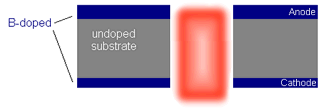
The all-diamond microplasmas are made by depositing a layer of conducting B-doped diamond on either side of a thick insulating undoped diamond layer, and then laser drilling a hole through the sandwich (see photo, below, right). Acid cleaning removes any graphitic residues in the cavity. The device is connected to a DC power supply and a discharge is struck in a suitable gas (e.g. helium) at pressures of a few 100 Torr, depending on the dimensions of the cavity. Our highest pressure microplasma to date operates at 9.5 atmospheres!

 |
|
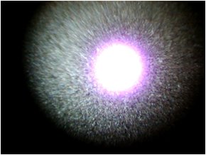
| A photograph of a 200 μm-diameter microplasma operating in helium gas at ~700 Torr. |
A movie of an 800 Torr microplasma operating at different voltages. |
Related Papers
- S. Mitea, M. Zeleznik, M.D. Bowden, P.W. May, N.A. Fox, J.N. Hart, C. Fowler, R. Stevens and N.St.J. Braithwaite, "Generation of microdischarges in diamond substrates", Plasma Sources Sci. Technol. 21 (2012) 022001.
- B.S. Truscott, C. Turner and P.W. May, "High-pressure dc glow discharges in hollow diamond cathodes", Plasma Sources Sci. Technol. 25 (2016) 025005. [doi: 10.1088/0963-0252/25/2/025005].