
Dr Paul May, S103A, email: paul.may@bris.ac.uk
An integrated circuit, or IC ('silicon chip') is a group of inseparably connected circuit elements fabricated onto, or within, a suitable substrate material. Most usual substrates are Si, or GaAs, in the form of thin wafers. Typical ICs may consist of up to ~20 layers of semiconducting materials, one on top of the other, forming a multilayer sandwich structure. Each layer is made of materials of precisely controlled electrical properties. The various layers are patterned such that the entire sandwich forms the various circuit elements (resistors, capacitors, etc.). These are finally linked by a patterned conducting layer (the interconnect), usually made of an Al alloy.
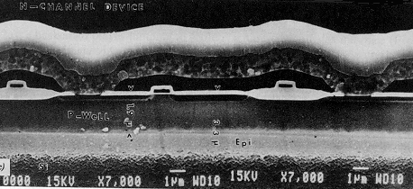
| Schematic diagram of a simple MOS transistor (right) and an SEM cross section of an actual one fabricated in Si (below). |
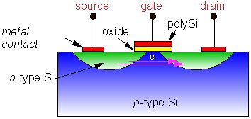 |
 The top figure shows one type of basic MOS transistor
(metal-oxide-semiconductor) - which is a bit of a misnomer since
nowadays the 'metal' gate is made from highly doped polycrystalline
Si - a good conductor. This acts as a fast switch: Normally
the electrical resistance through the Si between the source
and drain is so large that no current can flow. However,
if one applies a +ve voltage (normally +5 V) to the gate,
electrons from the bulk are attracted towards the gate and collect
behind the oxide layer. This accumulation of electrons now makes
the source-drain pathway conducting, and current can flow
between the two. As the gate voltage is varied, the current
between source and drain can be rapidly switched
on and off.
The top figure shows one type of basic MOS transistor
(metal-oxide-semiconductor) - which is a bit of a misnomer since
nowadays the 'metal' gate is made from highly doped polycrystalline
Si - a good conductor. This acts as a fast switch: Normally
the electrical resistance through the Si between the source
and drain is so large that no current can flow. However,
if one applies a +ve voltage (normally +5 V) to the gate,
electrons from the bulk are attracted towards the gate and collect
behind the oxide layer. This accumulation of electrons now makes
the source-drain pathway conducting, and current can flow
between the two. As the gate voltage is varied, the current
between source and drain can be rapidly switched
on and off.
We can now fabricate millions of such transistors on a simple wafer, laid out in specific patterns to allow logic gates (AND, NOR, etc.) to be arranged so as to form memory circuits, CPUs, device drivers, etc.
 The manufacturing process involves four main steps:
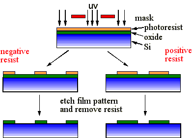
Etching involves removal of atoms from the films surface. These atoms will only be those that are exposed to the etching medium, and not those covered by a previously applied non-erodible photoresist mask. Thus the mask pattern is transferred into the underlying layer.
The etching process requires:
Previous generations of ICs used a wet etchant, e.g. an acid, but as the device dimensions dropped below ~5 µm in the mid-1980s, dry etching was developed in order to satisfy condition (2).
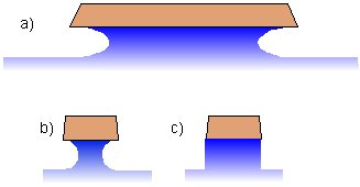
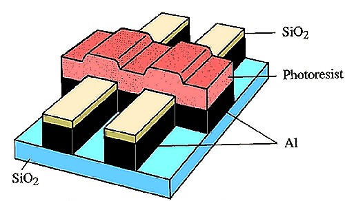
Diagram showing pattern transfer by etching. In isotropic (mainly chemical) etching, the mask etches laterally at about the same rate as vertically. This leads to mask undercutting and poor pattern definition. For large geometry circuits (a), the undercut is not significant compared to the dimensions of the feature. But as the feature sizes become similar to the etch depth (b), undercutting becomes a serious problem. Anisotropic etching (which is mainly a physical process, e.g. sputtering) gives better pattern transfer (c), and so is used in all modern etch processes. To obtain anisotropic etching, it became necessary to move away from the liquid-based acid etchants, and develop so-called 'dry etching' processes involving plasmas.
 Plasmas are often described as being the 4th state of matter, together with liquid, solid and gas. A plasma can be considered as an ionised gas consisting of a chemical soup of many types of species - positive and negative ions, electrons, neutrals, atoms, molecules, clusters, etc. Many different types of plasmas exist, from the high density ones found in stars, lightning strikes, and nuclear fusion reactors, to lower density ones found in the Northern Lights, and fluorescent lights. Indeed, some authors state that 99% of the universe is actually a plasma!
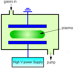
In the laboratory, plasmas can be easily generated by striking a high voltage (normally >1 kV) electrical discharge through a low pressure gas system. This can be achieved using a DC, AC, or more usually high frequency AC operating in the kHz-MHz (radio frequency, RF), or GHz (Microwave) regimes.
The discharge is started by an electron that originates from either (a) photoionisation of a neutral species by cosmic rays or background radiation, or (b) field emission caused by strong electric fields around a sharp point at the electrode surface. The applied electric field accelerates this electron causing it to undergo scattering collisions with gas molecules. As the electron accelerates, eventually it will possess enough KE to ionise a gas molecule through an inelastic collision. This releases another electron, which itself begins to accelerate, so initiating a cascade mechanism whereby other gas molecules are ionised in subsequent collisions.
To sustain the plasma, electrons must be generated at a rate which is large enough to offset the loss of electrons to the chamber walls, recombination with positive ions and/or electron attachment reactions. Another mechanism which generates electrons is bombardment of the electrode surfaces by energetic particles (ions or electrons), which causes high energy secondary electrons to be ejected back into the plasma.
 |
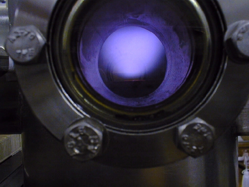 |
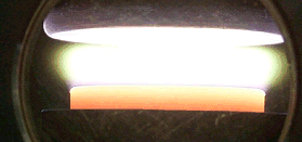
| An RF plasma showing the dark spaces at either electrode. | A working microwave plasma reactor in the Bristol CVD diamond lab. |
From the above, it can be seen that the gas pressure plays an important role. If the gas pressure is too low, electrons travel ballistically without colliding with sufficient gas molecules to sustain the cascade, and the plasma extinguishes. Conversely, if the gas pressure is too high, the electrons have too many low energy collisions, and cannot gain sufficient KE by acceleration to cause collisional ionisation. This can be partially overcome by using higher powers, but in general these two limitations ensure that most plasmas used in the semiconductor industry operate at pressures between ~1-500 mTorr (where 760 Torr = 1 atmosphere = ~1 bar = 101325 Pa).
AC discharges are preferred over DC-driven discharges in plasma systems for a number of reasons. First, as the frequency of the AC increases, the energy transfer into the discharge becomes more efficient, and becomes especially efficient at frequencies between ~100 kHz and 1 GHz, the RF regime. Also, in a DC discharge, charged particles from the plasma can accumulate on the substrate surface causing unwanted charging effects. By alternating the direction of the current flow sufficiently rapidly, these charging effects can be reduced. At RF frequencies this alternation is sufficiently rapid to almost completely eliminate charging effects, so allowing insulating materials (such as SiO2, Al2O3, etc), to be processed.
One problem, however, is that these frequencies are precisely those used for short wave radio communication, in say taxis, police cars, aircraft, etc! So to avoid interfering with these, the US Federal Communications Committee has decreed that certain frequencies (13.56 MHz, and 2.45 GHz) are to be set aside for plasma generation, and industry can emit vastly more power at these frequencies than at others - thus most plasma systems in industry operate at these frequencies, although with better screening technology some systems using other frequencies (e.g. 100 kHz, 90 MHz) are now making it onto the market.
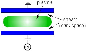 One of the features of a plasma is that whilst the bulk of the glow discharge remains at equipotential, most of the voltage applied between the electrodes is dropped across a small region surrounding any surface in contact with the plasma, especially the electrodes. This region is called the sheath (or 'dark space'), and we shall return to this in more detail in lecture 4. For now, the important thing to understand is that positive ions from the bulk of the plasma can be accelerated across this sheath and strike the electrode (and therefore the substrate) with high KEs. The voltage through which the ions are accelerated, and hence the KE with which they strike the substrate, depend upon many things, including the applied RF power, the gas pressure and the chamber geometry. As a consequence, many different plasma systems have been developed to exploit different ranges of these properties for different applications.
Plasma processes can be divided into different types, based on the nature of the gas-surface interactions. These can be (a) mainly chemical in nature, (b) mainly physical in nature, and (c) mixtures of the two.
This is largely chemical in action, and relies on the fact that with the right chemistry, surface atoms can be turned into gas phase molecules which can then be pumped away. A glow discharge plasma (usually RF) is used to generate reactive species, e.g. atoms, radicals and ions, from parent gases. These diffuse to the surface to be etched, form volatile products which then desorb from the surface and are pumped away.
A typical reaction would be:
CF4 ![]() F, CF, CF2, CF3, etc.
F, CF, CF2, CF3, etc.
Si(s) + 4F ![]() SiF4(g)
SiF4(g)
The chemistry has to be chosen carefully such that the etch product is a volatile species. For this reason most process gases in the semiconductor industry utilise halocarbons, such as CF4 or CF2Cl2 (which nowadays has become a cause for concern due to their environmental impact). For example, to etch Al (the material most IC interconnects are made from), chlorine-containing reactants are used (e.g. BCl3), since the etch product, AlCl3, is volatile under the low pressure process conditions. Fluorinated gases cannot be used for etching Al since AlF3 is a hard, crystalline material.
During etching of Si, often up to 8% O2 is added to the CF4 process gas since this (a) helps prevent the formation of PTFE polymers which could deposit onto the wafer sufrace and hinder etching, and (b) scavenges C to form CO and CO2, liberating all four F atoms, thus increasing the etch rate.
It is often desirable to be selective towards the underlying material, that is, to etch the top layer much faster than the lower layer. Again, suitable choice of chemistry allows this. For example if we wish to etch a Si layer on top of a SiO2 layer, without damaging the SiO2, we might employ chlorine-based chemistry at low power. Chlorine atoms which are generated in the plasma attack the Si lattice much more rapidly than the more strongly-bonded SiO2 lattice, and selectivities as high as 10:1 can be achieved. Note that if higher powers are used, ion bombardment, and with it physical sputtering, increases, so reducing the selectivity.
Advantages: can be highly selective to underlying layers, causes little damage to the photoresist or the lattice.
Nowadays plasma etching is mainly used for removing of the photoresist using O2-based plasmas (a process called ashing).
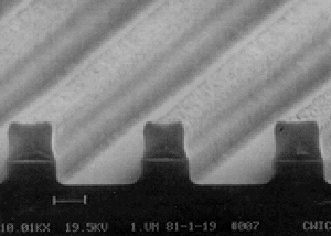 |
An ion beam milled set of tracks in Si. The photoresist is still in place. Notice the accurate pattern transfer from the mask into the Si, and also that the photoresist mask is beginning to show signs of damage and wear. |
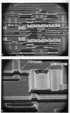 |
RIE combines the purely physical character of sputtering with the chemical nature of plasma etching. Reactive ions (e.g. CF3+, CCl3+) produced in a discharge are accelerated onto the wafer surface at high energies. In this case the wafer is placed onto the powered electrode, and high KEs are maintained by the use of low pressures (tens of mTorr). (left) An example of a complex multilevel circuit pattern created using RIE. |
RIE is now one of the most commonly used methods for etching semiconductor materials. This is because simultaneous bombardment of a substrate by both energetic ions and chemically reactive molecules or atoms can lead to etching which is substantially faster than would be predicted from simply adding together chemical etching + sputtering. This synergetic effect was first shown by Coburn and Winters in the etching of Si with separated and combined beams of XeF2 molecules and Ar+ ions.
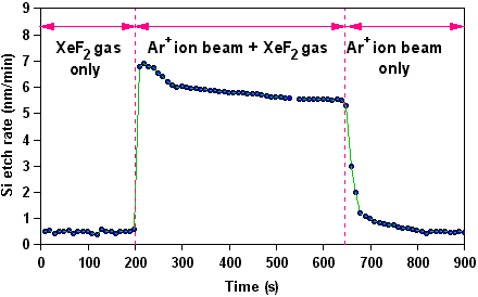 |
The Si etch rate as a function of separated and combined beams of XeF2 and Ar+. The etch rate of the combined beam is much greater than the sum of the two separate beams. |
Advantages: High anisotropy, good pattern definition, low damage, good selectivity to underlying layers.
Disadvantages: Still has some difficulty in etching 'problem' materials, e.g. Cu.
In order to increase etch rates, it is often necessary to work at high powers, but this can lead to significant substrate damage. To avoid this, we need to find a way to increase the plasma density without increasing the KE of the ion bombardment, in other words to decouple the power going into the plasma from the voltage dropped across the sheath. Some increasingly more common methods are magnetron ion etching (MIE), electron cyclotron resonance (ECR), and inductively coupled plasma (ICP) reactors. In MIE, carefully positioned magnets surrounding the RF chamber cause the electrons to travel in spiral paths. This greatly increases their path length, and so makes the probability of them striking a gas molecule much larger. The magnetic field therefore, can lower wall recombinations by confining the electrons to the centre of the plasma. Thus, high plasma densities can be obtained for low energy input. ECR is similar to MIE, except that it relies upon the interaction between the magnetic field and a plasma generated in a tuned microwave cavity.
In ICP, two RF power supplies are employed. One is capacitively coupled to one electrode, as before, whilst the other is inductively coupled through the walls of the chamber by wrapping the electrode in the form of a coil around it. This inductive component is the high power supply and is used to generate the plasma. The capacitively coupled RF supply is used to vary the sheath potential for the required application.
Disadvantages: Complexity and cost.
Advantages: Low powers, low damage, high anisotropy, high selectivity.
 Back to Introduction, forward to next lecture, or go to the Bristol Chemistry Home Page