 |
 |
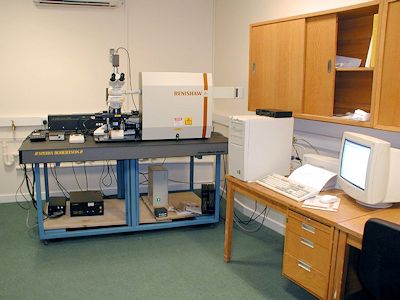
A Renishaw 2000 laser Raman spectrometer. This 3-wavelength system (UV at 325 nm, green at 514 nm and IR at 785 nm) allows the sp2/sp3 content of the films to be evaluated, as well as the quality and uniformity of the deposited films via a line-scan and 2D mapping facility. |
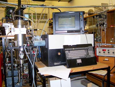
Optical emission spectroscopy equipment, both high and low resolution, for plasma diagnostics.. We also have a cavity ring-down spectroscopy system for measurements of absolute concentratins of the plasma as a function of position. |
 |
 |
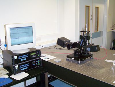
| An Ellipsometer - for measurements of film thickness and optical properties. This is more useful for obtaining the optical properties (refractive index and thickness) of DLC films rather than for crystalline diamond. |
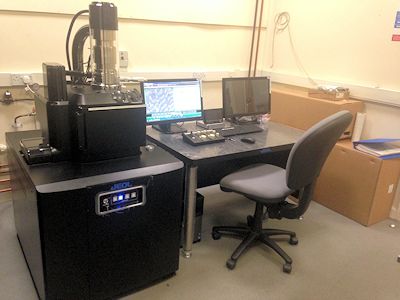
Scanning Electron Microscopy (SEM) and Transmission Electron Microscopy (TEM) analysis are available as part of the Electron Microscopy Facility (within the School of Chemistry. |
 |
 |
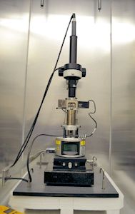
A Bruker Tunelling Atomic-Force Microscope (TUNA) system - for studies of surface morphology and conductivity is also available in the Electron Microscopy Facility. This allows near atomic-scale resoluion of surface features, as well as 3D surface maps overlaid with surface conductivity and electron emission profiles. |
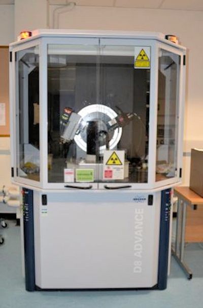
X-Ray Diffraction facilities - for determining crystal structures of solids and powders are available in the department. These can analyse thin films or powders, including nanodiamond. |
 |
 |
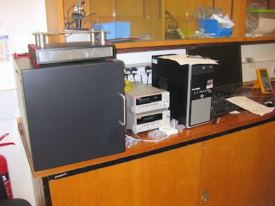
| A Hall-effect system - featuring a 1 T magnet for measuring n,p-type conductivity. The sample can be turned over to flip the direction of the magneic field to ensure accuracy of the readings. |
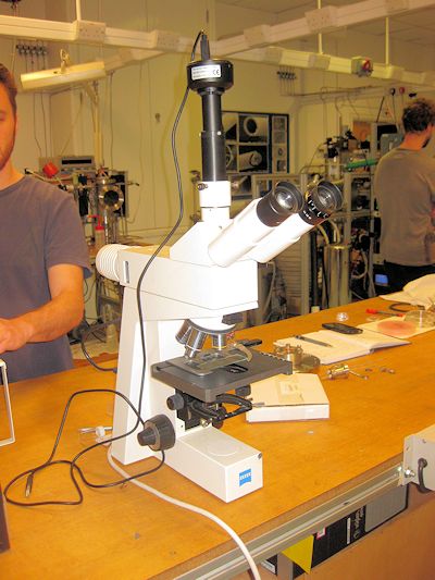
A Zeiss high-magnification (1200x) optical microscope with Normanksi interference filters. This high quality microscope allows superb images of micron-sized diamond crystallites, and has a camera attachment for hard-copies. |
 |
 |
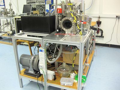
| A high-vacuum field-emission testing station. This uses a high voltage probe to extract electrons from the surface of a grounded diamond substrate, and can measure the voltage required to do this as a function of electrode-substrate separation. |
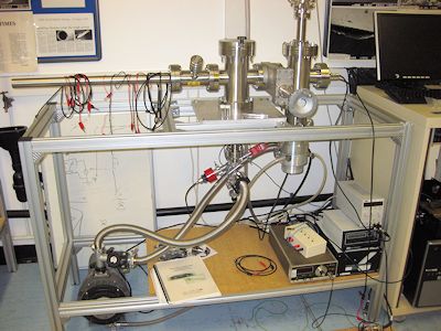
A high-vacuum testing station for measuring the secondary electron yield from a diamond surface. Various configurations can be sued to measure the yeield in reflection or transmission modes, and as a function of primary electron energy supplied by a variable power electron gun. |
 |
 |
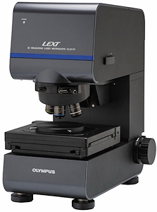
| Olympus LEXT OLS5100 - confocal laser microscope for surface analysis. A 405 nm laser captured images and surface features with zoom between 10x and 100x objectives (100 nm resolution), generating 3D acquisitions of surface characteristics and 2D surface profiles. For larger areas, stitching of multiple analysed areas allowed for more detailed analysis of the entire sample area. |
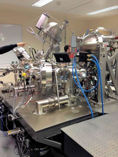
NanoESCA system - capable of a multitude of UHV in situ experiments, including XPS, LEED, PEEM and monolayer evaporation. We also have an Omicron high-resolution STM and Kelvin probe system - for measuring surface work functions. |
