 Production of B-Doped Diamond Films for use as Inert Electrochemical Electrodes
Highly boron-doped diamond (BDD) exhibits electrical conductivity comparable to that of many metals, thus making it suitable as an electrode material for electrochemical redox reactions. Compared to conventional electrodes made from gold, platinum, or glassy carbon, those composed of or coated with BDD offer numerous advantages for electrochemistry (see cyclic voltammetry comparisons, right).
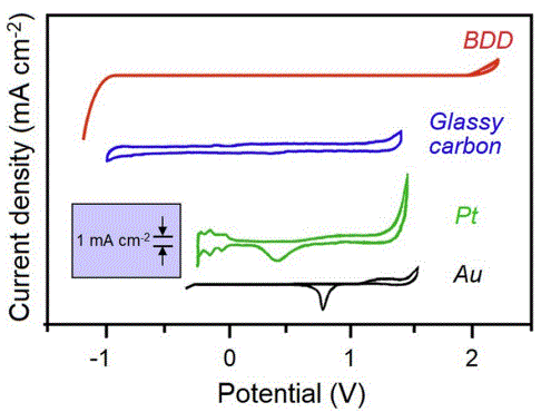
- Their primary benefit lies in the significantly broader operating range, enabling operation within potentials ranging from –1 to +1.8 V. This facilitates the detection or analysis of redox species typically beyond the operating range of conventional electrodes.
- The signal response is flat within this operating window, which means there is virtually no background or capacitance, allowing the BDD electrodes to be highly sensitive to small changes in analyte concentration. BDD electrodes are therefore able to detect compounds at nanomolar [i.e., parts per billion (ppb)] concentrations, even when chemically similar species are also present.
- BDD electrodes are chemically inert and resistant to corrosion under conditions of elevated temperatures and pressures, as well as in environments hostile to other electrode materials.
- Diamond is also recognised as being bioinert, i.e., it does not elicit immune responses, including inflammation or rejection in living cells, allowing it to be used in various biochemical environments or inside living organisms.
- Diamond electrodes are highly resistant to fouling, and also, in many circulstances, they can be self-cleaned by applying a high reverse current for a short time.
We are depositing boron-doped CVD diamond films for use as inert electrodes in a range of electrochemical applications. Boron doping is achieved using B2H6 gas at concentrations of a few 100 ppm in the usual CH4/H2 gas mixture. Diamond films can be made with conductivity ranging from highly insulating, through various degrees of semiconductivity, to fully metallic, depending upon the B-doping level we choose. Electrochemistry experiments using these films, and with films of nanodiamond, are performed with the help of David Fermin's group.
Large-surface-area electrodes
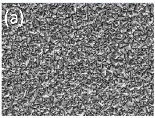
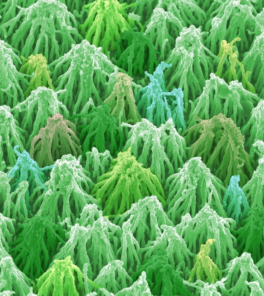
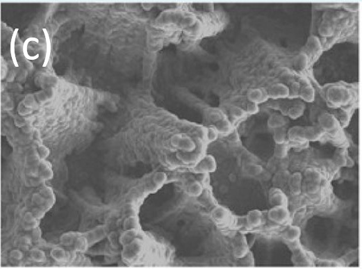
Another useful property of CVD diamond electrodes is that they can be patterned into various micro- or nanosized structures, for example, nanowires, foams, fibres, and needles. Such nanostructures can increase the active electrochemical surface area by up to 1000 times compared to flat electrodes, together with an associated huge increase in sensitivity.
 |
 |
 |
| (a) 'Flat' nanocrystalline diamond | (b) (False colour) diamond 'teepee' structures formed by depositing a thin BDD coating onto vertically aligned CNTs |
(c) 'Honeycomb' structures by overgrowing CNT structures with BDD. |
'Black diamond' electrodes
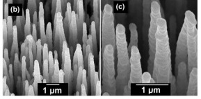
Black silicon is a synthetic nanostructured material that contains high-aspect-ratio nanoprotrusions, such as nanospikes or nanoneedles, on its surface produced through plasma etching. Coating these needles in a thin conformal layer of CVD diamond produced ‘black diamond’, which is more mechanically robust while still retaining its anti-microbial properties. Black diamond is being studied here for its use as antimicrobial coatings, but when boron doped, it also acts as an excellent high-surface-area electrode.
 |
 |
(b,c) SEM images of nanostructured BDD needles with an electrochemically active area ~220 times larger than that of a flat diamond electrode.
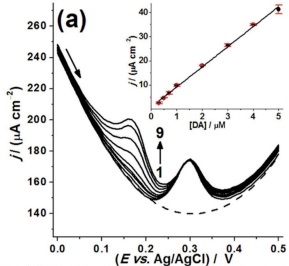
On the right (a) are the differential pulse voltammograms recorded for different concentrations (plots 1–9; 0–5 μM) of dopamine (DA) in the presence of 30 μM uric acid — a chemically similar analyte. Inset: Current density j / (mA cm-2) vs. concentration of dopamine (μM) showing a linear response with concentration.
 Bespoke nanopatterned electrodes
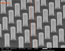
Black silicon is rather difficult to fabricate reproducibly. As such, we are currently working on ways to replace black Si with bespoke patterned nanocolumns of Si (as shown in the right-hand pictures), produced by nanolithography followed by RIE etching. The optimum would be to make tall (h = 2 μm) closely spaced (p = 200 nm pitch), thin (w = 100 nm wide) columns in a dense grid structure, similar to that of black Si but more reproducible and controllable. All three parameters, h, p and w are controllable, allowing a range of different grid sizes to be tested. These nanocolumns are then coated with diamond, and then tested for their electrochemical performance. Preliminary tests show such electrodes can have close to 100 times the electrode area of a flat electrode.
Decorating Electrodes with Metal Nanoparticles
These large-surface-area, 3D nanostructured diamond electrodes lend themselves nicely to being decorated with catalytic metallic nanoparticles. The next stage of this project will be choose a suitable metal nanoparticle (Fe, Ni, Pt, etc) for a specific chemical application, such as water splitting or CO2 valorisation, apply these to the BDD electrodes, and then determine if the chosen chemical reactions can be enhanced by the combination of nanoparticles and high-surface-area. Watch this space...
Related Papers
- M.N. Latto, D.J. Riley and P.W. May, "Impedance Studies of Boron Doped CVD Diamond Electrodes" Diam. Relat. Mater., 9 (2000) 1181-1183.
- N.A. Fox, M.J. Youh, W.N. Wang, J.W. Steeds, H-F. Cheng, I-N. Lin, "Impedance Studies of Boron Doped CVD Diamond Electrodes" Diam. Relat. Mater., 9 (2000) 1263-1269.
- M. Alexander, M.N. Latto, G. Pastor-Moreno and D.J. Riley, "The Influence of Surface Termination on the Electrochemical Properties of Boron-doped Diamond", Proc. 7th Int. Symp. Diam. Maters., PV 2001-25 (2001) pp.54-65
- G. Pastor-Moreno and D.J. Riley, "Electrochemical Studies of Moderately Boron Doped Polycrystalline Diamond in Non-Aqueous Solvent", Electrochimica Acta, 47 (2002) 2589-95
- G. Pastor-Moreno and D.J. Riley, "The influence of surface preparation on the electrochemistry of boron doped diamond: A study of the reduction of 1,4-benzoquinone in acetonitrile", Electrochem. Comm., 4 (2002) 218-221
- M.S. Alexander, M.N. Latto, P.W. May, D.J. Riley and G. Pastor-Moreno, "A simple route to Ohmic contacts on low boron-doped CVD diamond", Diamond Relat. Mater., 12 (2003) 1460-1462.
- M.N. Latto, G. Pastor-Moreno, D.J. Riley, "The Influence of Doping Levels and Surface Termination on the Electrochemistry of Polycrystalline Diamond", Electroanal., 16 (2004) 434-441
- H. Zanin, P.W. May, E. Saito, J. P. B. Machado, G. Martins, V.J. Trava-Airoldi and E. J. Corat, "Effect of multi-walled carbon nanotubes incorporation on the structure, optical and electrochemical properties of diamond-like carbon thin films", J. Electrochem. Soc. 161 (2014) H290-H295. [DOI: 10.1149/2.011405jes]
- T.A. Silva, H. Zanin, P.W. May, E.J. Corat, and O. Fatibello-Filho, "Electrochemical Performance of Porous Diamond-like Carbon Electrodes for Sensing Hormones, Neurotransmitters, and Endocrine Disruptors", ACS Appl. Mater. and Interfaces 6 (2014) 21086-21092. [doi: 10.1021/am505928j]
- H. Zanin, P. W. May, D. Fermin, D. Plana, S. M. C. Vieira, W. I. Milne and E. J. Corat, "Porous boron-doped diamond/carbon nanotube electrodes", ACS Applied Materials & Interfaces 6, (2014) 990-995.
- H. Zanin. P.W May, R.L Harniman, T. Risbridger, E.J. Corat, D.J. Fermin, "High surface area diamond-like carbon electrodes grown on vertically aligned carbon nanotubes", Carbon 82 (2015) 288-296.
- H. Zanin, C.M.R. Rosa, N. Eliaz, P.W May, F.R. Marciano, and A.O. Lobo, "Assisted deposition of nano-hydroxyapatite onto exfoliated carbon nanotube oxide scaffolds", Nanoscale 7 (2015) 10218-10232. [doi: 10.1039/C4NR07317G].
- P.W. May, M. Clegg, T.A. Silva, H. Zanin, O. Fatibello-Filho, V. Celorrio, D.J. Fermin, C.C. Welch, G. Hazell, L. Fisher, A. Nobbs, B. Su, "Diamond-coated ‘black silicon’ as a promising material for high-surface-area electrochemical electrodes and antibacterial surfaces", J. Mater. Chem. B. 4 (2016) 5737-5746. [doi: 10.1039/c6tb01774f]
- A.C. Peterlevitz, P.W. May, R.L. Harniman, J.A. Jones, H.J. Ceragioli, H. Zanin, "Fast electron transfer kinetics on novel interconnected nanospheres of graphene layers electrodes", Thin Solid Films, 616 (2016) 698-702. [doi: 10.1016/j.tsf.2016.09.044]
