
 Field Emission from Diamond for use in Cold Cathode Devices
For some materials, such as diamond, the conduction band minimum (CBM) lies higher in energy than the vacuum level. This uncommon situation is known as negative electron affinity (NEA). With NEA, any electrons located in the CB experience no emission barrier to escape the surface. As such, bulk electrons residing in the VB (or in mid-band-gap states as a result of p- or n-type doping), only need to be excited into the CB for emission to take place. Consequently, materials with NEA require far less photon or thermal energy for electron emission, and so are promising candidates for next-generation electron-emission applications.
One method to extract these electrons is called Field Emission, and involves using a high potential difference. Diamond's NEA means that this extraction voltage can be significantly lower than for other materials. This makes possible applications such as microelectronic devices, sensors, and flat-panel displays.
 |
 |
| Field emission is when a high potential is used to drag electrons out of a material. The electric field can be concentrated around disparities on the flat surface, such as grain boundaries, defects or impurities, or nanoengineered needles/tips. The enhanced field at these points lowers the barrier for emission and so greatly increases the current. | A schematic diagram of how a diamond-based cold-cathode field-emitting display might be fabricated. Elelectrodes are patterned around conducting diamond tracks, and a high voltage causes electrons to be emitted and accelerated upwards. These high-energy electrons strike a phosphor-coated plate creating light, which would form a pixel in a display. |
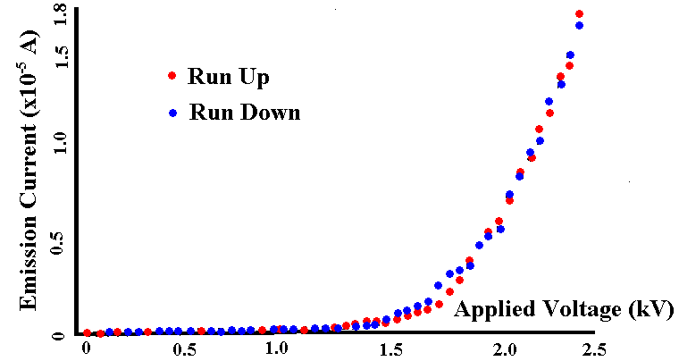
We previously worked on measuring the I-V characteristics of diamond films grown under a number of different deposition conditions, and by a variety of diverse methods, such as polycrystalline and nanocrystalline CVD diamond made by Hot Filament and Microwave reactors, diamond-like carbon (doped and undoped) made by RF plasma deposition methods, and ta-C films made by laser ablation of graphite. Examples of the IV curves are given below.
 |
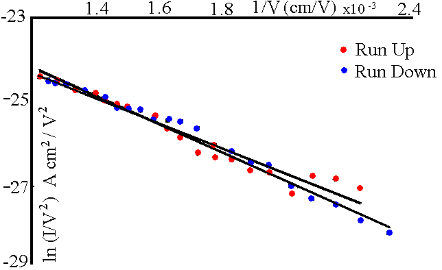 |
| Restricted Fowler-Nordheim plot from the electron emission of the MW CVD sample. | I-V curve for field emission from a Microwave Plasma-grown CVD diamond film, at an electrode distance of 30 μm. The 2 curves were taken for increasing voltage and decreasing voltage to check for hysteresis. |
Field emission from Diamond/CNT compositesA few years ago we developed a process to make diamond-coated carbon nanotubes (CNTs). This involved electrospray seeding 'forests' of vertically aligned multiwall CNTs which caused the CNTs to clump together and join at their tips to produce 'teepee' structures. Once coated with a thin layer of B-doped CVD diamond (photo, right), these composite teepees show excellent field emission characteristics with hugely extended lifetimes. |
 False-colour SEM image of the teepees. |
Studies of the Mechanism of Field Emission from Granular Diamond Films
We used PEAKFORCE AFM to study where the electrons were emitted during field emission. In this process an AFM tip with nm resolution is passed over a diamond film while applying a voltage sufficient to cause field emission. The locations from where electrons emit then reveal themselves as bright areas, while the non-emitting areas remain dark. Thus, both topological and electron emission data can be overlaid, showing the emission sites. The results showed clearly that field emission originates from the grain boundaries of polycrystalline films, and not the sharp tips as previously believed. Thus, for optimal field emission we require diamond films with many grain boundaries, such as UNCD, and these do not need to be patterned into tips or needles as flat films with work just as well.
 |
 |
Measured emission current overlaid on their corresponding measured topographic image for undoped NCD films. The images have been colour-scaled from dark–blue (low emission) to light–blue (high emission). The left-hand image is a large-area scan 10 μm × 10 μm, while the right-hand image is images of a smaller region (3 μm × 3 μm) revealing more detail of the grain structure. Electron emission is evident from grain boundaries at all grain sizes. |
Related Papers
- N.A. Fox, S. Mary, T.J. Davis, W.N. Wang, P.W. May, A. Bewick, J.W. Steeds and J.E Butler, "Field Emission Studies of Boron-Doped CVD Diamond Films following Surface Treatments", Diamond Relat. Mater. 6 (1997) 1135-42.
- N.A. Fox, W.N. Wang, T.J. Davis, J.W. Steeds and P.W. May, "Field Emission Properties of Diamond Films of Different Qualities", Appl. Phys. Lett., 71 (1997) 2337-39.
- P.W. May, J.C. Stone, M.N.R. Ashfold, K.R. Hallam, W.N. Wang and N.A. Fox, "The Effect of Diamond Surface Termination Species upon Field Emission Properties", Diamond Relat. Mater. 7 (1998) 671-676.
- P.W. May, S. Höhn, W.N. Wang and N.A. Fox, "Field Emission Conduction Mechanisms in Chemical Vapour Deposited Diamond and Diamondlike Carbon Films", Appl. Phys. Letts. 72 (1998) 2182-2184.
- P.W. May, S. Höhn, M.N.R. Ashfold, W.N. Wang, N.A. Fox, T.J. Davis and J.W. Steeds "Field Emission from Chemical Vapor Deposited Diamond and Diamond-like Carbon Films: Investigations of Surface Damage and Conduction Mechanisms", J. Appl. Phys. 84 (1998) 1618-1625.
- P.W. May, S. Höhn, M.N.R. Ashfold, W.N. Wang, N.A. Fox, T.J. Davis and J.W. Steeds "Investigations of Surface Damage and Conduction Mechanisms During Field Emission from CVD Diamond and DLC Films", Diamond Films and Technol. 8 (1998) 237-247.
- P.W. May, M-T. Kuo and M.N.R. Ashfold, "Field Emission Conduction Mechanisms in Chemical Vapour Deposited Diamond and Diamondlike Carbon Films", Diamond Relat. Mater. 8 (1999) 1490-1495.
- M.T. Kuo, P.W. May, A. Gunn, J.C. Marshall, M.N.R. Ashfold and K.N. Rosser, "Field Emission Studies of Nitrogen-Doped Diamond-like Carbon Films Deposited using CH4/N2/Ne and CH4/NH3/Ne RF Plasmas" Int. J. Mod. Phys. B: Condensed Matter Phys. 14 (2000) 295-300.
- M-T. Kuo, P.W. May and M.N.R. Ashfold, "Field Emission studies of low temperature thermal-annealling of nitrogen-doped hydrogenated amorphous carbon (a-C:H:N) films", I 10 (2001) 889-894.
- M.T. Kuo, P.W. May and M.N.R. Ashfold, "Field emission site density study of hydrogen-free amorphous carbon films", Diamond Relat. Mater. 11 (2002) 1422-28.
- S.A. Furkert, A. Wotherspoon, D. Cherns, N.A. Fox, G.M. Fuge, P.J. Heard, S.P. Lansley, "Field emission observed from metal-diamond junctions revealed by atomic force microscopy", Appl. Phys. Letts., 90 (2007) 242109.
- Y. Zou, P.W. May, S.M.C. Vieira, N.A. Fox, "Field emission from diamond-coated multiwalled carbon nanotube 'teepee' structures", J. Appl. Phys. 112 (2012) 044903.
- H. Zanin, P.W. May, M.H.O.M. Hamanaka, E.J. Corat, "Field emission from hybrid diamond-like carbon and carbon nanotube composite structures", ACS Applied Materials & Interfaces 5 (2013) 12238-12243.
- V. Chatterjee, R. Harniman, P.W. May, P.K. Barhai, "Direct observation of electron emission from the grain boundaries of chemical vapour deposition diamond films by tunneling atomic force microscopy", Appl. Phys. Lett. 104 (2014) 171907. [doi: 10.1063/1.4875059]
- R.L. Harniman, O.J.L. Fox, W. Janssen, S. Drijkoningen, K. Haenen, and P.W. May, "Direct observation of electron emission from grain boundaries in CVD diamond by PeakForce-controlled tunnelling atomic force microscopy", Carbon 94 (2015) 386-395. [doi: 10.1016/j.carbon.2015.06.082].
- R. Harniman, P.W. May, O.J.L. Fox, "Direct observation of electron emission from CVD diamond grain boundaries by tunnelling atomic force microscopy independent of surface morphology", Diamond Relat. Mater. 80 (2017) 147-152.