 Growth of diamond on GaN
Gallium nitride (GaN) electronic devices are in high demand for high-power, high-frequency applications due to their outstanding properties. For instance, GaN high electron mobility transistors (HEMTs) can be used as transmitter base-stations for mobile communications (e.g. 4G, 5G or 6G mobile phone networks). However, at high powers and/or high frequencies, these devices become extremely hot resulting in degradation of device performance and a huge decrease in their reliability. For GaN HEMTs to play a part in the drive for 5G communications and beyond, improved thermal management is a necessity for the devices to operate at the required power densities with an acceptable lifetime. One solution to this is to attach the GaN device to a high-thermal-conductivity material which can rapidly transfer the localised heat to an external cooling system or radiator. Commercial GaN devices currently use a technology based on thin films (~2 μm thick) of GaN deposited onto a silicon carbide (SiC) wafer with a thin nucleation layer. Although the thermal conductivity values for bulk GaN (160 W m-1 K -1) and SiC (~420-490 W m-1 K -1) are reasonably high, the nucleation layer and the resulting microstructure near to the interface can cause a significant barrier for heat to travel from the GaN device to the SiC substrate. Replacing the conventional SiC substrates with a high-conductivity substrate, such as diamond (2000 W m-1 K -1),allows for a 3 times increase in RF output powerdensity and greatly improved device performance and lifetime. |
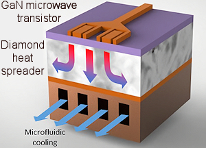
 A proposed high-pwer GaN microwave device fabricated on top of a thick CVD diamond heat spreader, which transfers heat to a microfluidic cooler. |
However, depositing diamond onto GaN is tricky for a number of reasons. First, diamond CVD utilises high temperatures (typically 800 °C and above) and a gaseous environment rich in atomic hydrogen. Under these conditions, atomic hydrogen can etch GaN (to form NH3 and liquid Ga), preventing diamond deposition. This etching can be prevented if the GaN surface is seeded with nanodiamond (ND) sufficiently densely that the lateral diamond growth rate exceeds the etch rate. In this case, a protective diamond layer grows to cover the GaN surface before significant etching can occur. Even with these measures, the interface between GaN and diamond is rather weak because Ga does not form a carbide. Thus, the diamond adheres to the GaN mainly via weak van der Waals interactions, rather than strong covalent bonds, making it prone to delamination. This becomes a serious problem when cooling the samples down from the diamond CVD temperatures, because GaN has a room-temperature thermal expansion coefficient that is 28% larger than that of diamond. Uponcooling, the GaN will contract back to its room-temperature volume while the diamond to which it is bonded contracts far less. This causes compressive stresses to be developed in the diamond layer, leading either to unwanted bowing of the sample or to delamination of the entire diamond layer. Moreover, the thermal conductivity of the ND nucleation layer (which can be ~100 nm thick) is very poor, creating a thermal bottleneck at the GaN/diamond interface.
To overcome some of these growth and adhesion problems, thin buffer layers of SiC or SiN have been used between the diamond and GaN. However, these layers often have poor thermal conductivity, and so themselves create a thermal bottleneck. A workable compromise is to use AlN as the barrier layer, and recent work showed that diamond growth onto AlN is a possible pathway forward.
 |
 |
 |
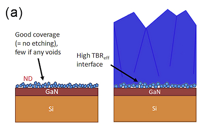
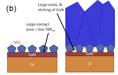
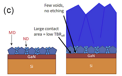
Schematic diagram explaining the rationale for two-step seeding. The left-hand panels show the seeding method, while the right-hand panels are after subsequent diamond CVD. (a) Seeding with ND alone provides good surface coverage with few, if any, surface areas exposed. Upon diamond growth, there is little or no etching of the GaN surface, but the nucleation layer of ND has a high TBReff. (b) Conversely, seeding with only microcrystalline diamond (MD) provides large-surface-area contacts and therefore efficient heat transfer, but the exposed GaN surface creates voids at the interface as well as suffering etch damage during diamond CVD. The voids reduce the adhesion at the interface making the film more prone to delamination, as well as increasing the TBReff hugely. (c) Two-step seeding (MD followed by ND) allows the benefits of both- a large contact area and therefore low TBReff, plus very few voids and no etching. |
Our work - Mixed size seeding
To solve some of these problems, we used a mixture of microdiamond and nanodiamond seeding, followed by CVD diamond growth, onto thin layers of both GaN and AlN on Si substrates. This was part of UK project called GaN-DAME which was multi-university project from 2018-23 to try to solve this issue. We found that diamond films grown on a thin AlN barrier layer on GaN were adherent and robust, while a novel two-step mixed-seeding method (see figure, above) gave effective thermal boundary resistance values (TBReff) < 6 m2 K GW-1 that were 30 times smaller than for films grown under identical conditions but using nanodiamond seeding alone. Such remarkably low thermal barriers obtained with the mixed-seeding process offer a promising route for fabrication of high-power GaN HEMTs using diamond as a heat spreader with an AlN interlayer.
Example papers
- P.W. May, H.Y. Tsai, W.N. Wang and J.A. Smith, "Deposition of CVD Diamond onto GaN", Diam. Relat. Maters. 15 (2006) 526-530.

- E.J.W. Smith, A.H. Pirach, D. Field, J.W. Pomeroy, G.R. Mackenzie, Z. Abdallah, F.C-P. Massabuau, A.M. Hinz, D.J. Wallis, R.A. Oliver, M. Kuball, P.W. May, "Mixed-Size Diamond Seeding for Low-Thermal-Barrier Growth of CVD Diamond onto GaN and AlN", Carbon 167 (2020) 620-626.
 [DOI: 10.1016/j.carbon.2020.05.050]
