
 Patterning of CVD Diamond films
In order to make devices, displays, sensors, etc, out of diamond films, it is first necessary to pattern the film in some way. Patterned diamond films are being produced at Bristol using a number of techniques, including selective nucleation, lift off, and dry etching methods. The following SEM photos show examples of a patterned diamond film produced by selective nucleation. The Si wafer was first coated on oxide, and then patterned using standard photolithography and dry etching techniques to expose areas of Si. The wafer was then abraded, and the oxide mask stripped off in HF. Subsequent CVD produced diamond growth on the abraded areas preferentially over the unabraded areas. The resolution of this method appears to be around 2-5 μm. Some patterned films can be seen in the SEM images below.


CVD Diamond Membranes
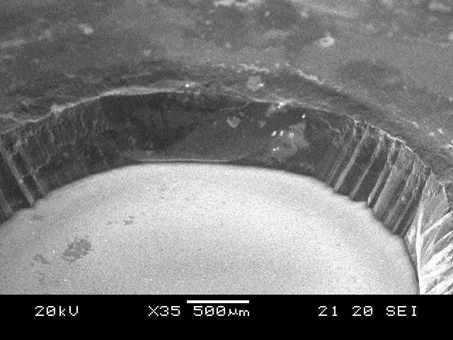
By etching away selective areas of the Si substrate using hot KOH, a supported membrane, or window, made from CVD diamond could be made. Examples of these are seen in the photo and SEM, below. The largest we made was a window 5 mm in diameter and 300 nm thick, which has an aspect ratio of ~20,000! To put this in context, this would be the equivalent of a standard glass windowpane (say 3 mm thick) with a diameter of 50 m!
 |
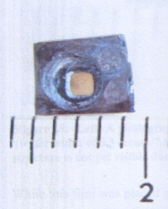 |
| SEM image of the back side of a 0.5 μm-thick diamond membrane, showing the etched Si sidewall. | Photograph of the whole membrane, with a scale bar in inches. The Si wafer is 0.4 inches, and the membrane is ~0.1 inches (2.5 mm) in diameter. |
By using special seeding methods utilising detonation nanodiamond and electrospray we can now make a monolayer of close-packed seeds on a Si surface. CVD for only a few minutes yields continuous diamond films that are only a few 10's of nm thick over areas up to 1 square cm. Such membranes can be used as diamond windows, or for measurements of secondary electron emission in transmission mode.