 Secondary-electron emission from diamond
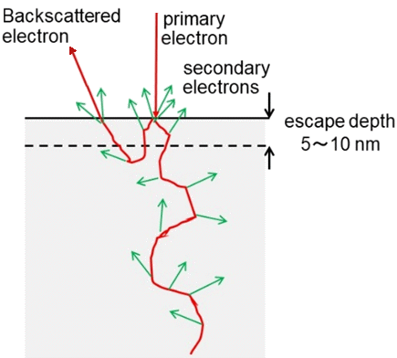
 When a primary high-energy beam of electrons (red) strikes a surface, they can travel deep into the material, striking bulk electrons, and transferring momentum to them. The primary electrons slow down and perhaps change direction, having many more collisions until they eventually either stop deep in the bulk, or re-emit through the surface as a backscattered electron. The knock-on electrons can themselves travel through the material and strike further electrons, resulting in a cascade of electrons with a range of energies and directions. Some of these electrons are travelling in a direction which takes them towards the surface and may be emitted into vacuum as secondary electrons (green). The ratio of secondary emitted electrons to primary incoming electrons is called the secondary electron yield, SEY, and depends, among other factors, upon the size of the energy barrier that the bulk secondary electrons need to overcome to escape into vacuum.
Diamond is a very unusual material, in that if its surface is terminated with a (sub)monolayer of certain species, such as H, Si and most metals, it exhibits so-called negative electron affinity (NEA). This means that electrons can be emitted from its surface without having to overcome an energy barrier, while the number of electrons emitted (the emission current) is greatly increased.
As a result, natural and CVD diamond have been measured as having SEE values as high as 80, although more typical values are ~10. This means that 10 slow electrons are emitted for every 1 fast incident electron. These emitted electrons can be accelerated using a potential difference to strike a second diamond surface, giving rise to even more electrons. Often, several stages of acceleration are used with progresively increasing voltages, to multiply the number of electrons by maybe 1 million times - sufficient to detect as an electrical current. This is the basis for electron multiplication as used in photomultiplier tubes and night-vision goggles.
Advantages of diamond
- High gain: because of the high SEY or gain of diamond, fewer multiplication stages are required to obtain sufficient electrons to detect as a current, making the devices smaller and cheaper.
- Fast response: The electron emission process occurs on a fs timescale, suggesting that extremely fast-response photomultiplier tubes can be fabricated using diamond.
- Long lifetime: The diamond surface should be inert and so devices should have longer lifetimes than current ones.
Reflection or Transmission mode?
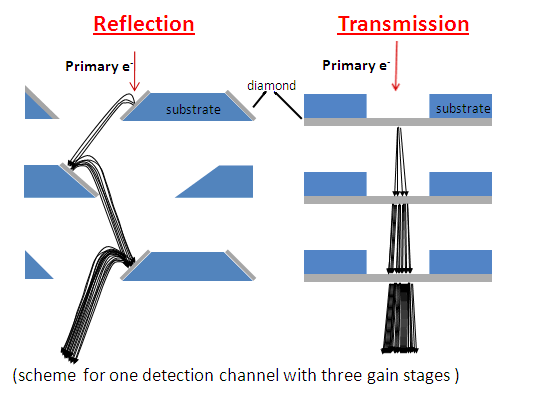
When electrons are emitted from the same surface struck by the incident electron beam, this is called reflection mode. Multiplication in this case occurs by having the surfaces at an angle to the incident beam, with the second surface below this and to one side, in a so-called 'Venetian blind' structure (see figure below, left). Alternatively, if the sample is thin enough, electrons are emitted from the opposite surface to that struck by the incident electron beam - this is transmission mode (see diagram, below right). This mode allows line-of-sight multipliers to be fabricated, which can be simpler than the Venetian blinds. However, it relies on fabricating thin membranes of diamond which are ~100 nm thick.

Measurements of SEY
In a collaboration with Jon Lapington's group at the University of Leicester, Photek and other partners, we measured the SEY for different types of diamond as a function of doping, surface termination, crystal size, etc, with the aim of fabricating a demonstrator high-gain, fast-response photomultiplier system. Both reflection and transmission modes were investigated using a home-built system.

Some results are shown in the figures below.
 |
 |
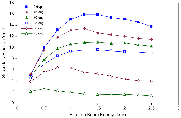
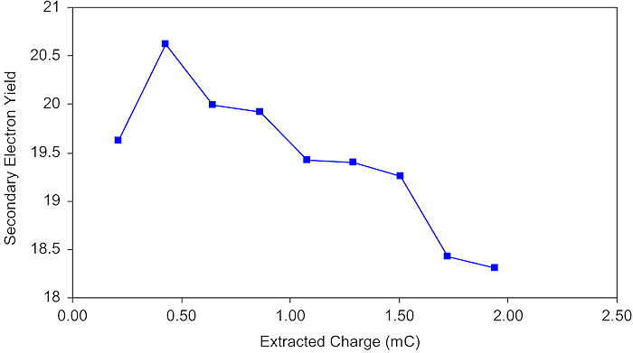
| Measured SEY versus energy for hydrogen-terminated B-doped CVD diamond deposited on molybdenum, with the electron beam at various angles of incidence. | The degradation of SEY with increasing electron beam charge. |
The peak of SEY occurs at a primary electron energy of ~1 keV, as expected from previous reports. For our B-doped MCD films the maximum SEY was around 20, although other films gave values as high as 45. The disapointing result was the rapid permanent degradation of the SEY with extracted charge, i.e. the total emission current, as this means the lifetime of any electron-multiplication device would be very low. This degradation is a result of the desorption of the H termination on the surface of the diamond, probably due to the cumulative electron impacts with the outgoing secondary electrons. One way to solve this is to use more robust surface terminations, such as metal or metal oxide (sub)monolayers - and these would bring the added advantage of a larger NEA. We are currently working on identifing such a surface.
Related Papers
- J.S. Lapington, P.W. May, N.A. Fox, J. Howorth, JA. Milnes, "Diamond dynodes create new breed of photon detectors", Laser Focus World (Sept 2008).
- J.S. Lapington, D.P. Thompson, P.W. May, N.A. Fox, J. Howorth, J. Milnes, V. Taillandier, "Investigation of the secondary emission characteristics of CVD diamond films for electronamplification", Nucl. Instr. Methods Phys. Res. A, 610 (2009) 253–257.
- R. Vaz, P.W. May, N.A. Fox, C.J. Harwood, V. Chatterjee, J.A. Smith, C.J. Horsfield, J.S. Lapington and S. Osbourne, "Measurement of the secondary electron emission from CVD diamond films using phosphor screen detectors", JINST 10 (2015) P03004
