 Electron emission from diamond surfaces
Many advanced technological applications exploit the controlled emission of electrons from a surface for their operation. These include, for example, emissive flat-panel displays, spacecraft ion engines, high-power microwave amplifiers, X-ray sources, electron microscopy, and electron-beam lithography techniques.
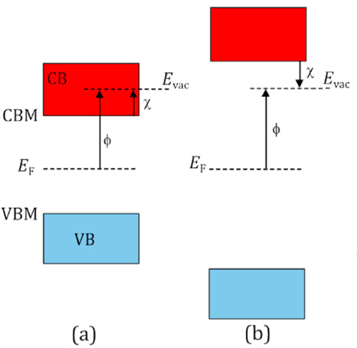
For an electron to be emitted from a surface, it must possess sufficient energy to overcome the potential barrier situated at the interface between the surface and the external medium, which is usually a vacuum, but could be air or water. This potential barrier � the work function, φ � is defined as the energy difference between the Fermi level (the electrochemical potential of electrons inside the material) and that of the vacuum level. For wide-band-gap semiconductor materials operating at normal temperatures, the conduction band (CB) is usually empty of electrons while the valence band (VB) is partially or fully occupied. The two bands are separated by an energy band gap of a few eV (e.g., 1.1 eV for Si and 5.47 eV for diamond). This means φ for most metals and semiconductors is also typically several eV. For most materials, there is also an extra energy barrier for electrons i the CB to overcome before they can leave the surface and be emitted into vacuum. This barrier is called the electron affinity, χ, and can be several more eV. Hence, either UV photons or temperatures >1500 K are required to provide sufficient energy to emit electrons located at the Fermi energy in the VB directly into the vacuum or to excite them into the CB to be subsequently emitted from there. |
 |
Schematic diagram illustrating the electron affinity, χ, and its relationship to the workfunction, φ, in relation to a fixed vacuumlevel Evac. VB is the valence band and VBM the valence band maximum, CB is the conduction band and CBM is the conuction band minimum, while EF is the Fermi level. (a) Positive electron affinity (PEA) which is the case for mosr materials. (b) Negative electron affinty (NEA) which occurs in diamond with suitable surface termination. |
However, for some semiconductors and insulators, such as diamond, an alternative emission pathway is possible if the conduction band minimum (CBM) lies higher in energy than the vacuum level. This uncommon situation is known as negative electron affinity (NEA). With NEA, any electrons located in the CB experience no emission barrier to escape the surface. As such, bulk electrons residing in the VB (or in mid-band-gap states as a result of p- or n-type doping), only need to be excited into the CB for emission to take place. Consequently, materials with NEA require far less photon or thermal energy for electron emission, and so are promising candidates for next-generation electron-emission applications.
Diamond possesses an NEA surface when it is terminated with certain electropositive chemical species. As mentioned above, the most common species found on the surface of natural and CVD diamond is hydrogen. The small difference in electronegativity between carbon and hydrogen creates a surface dipole, with the positive charge outermost, lowering the emission barrier and establishing the NEA. As a consequence, electrons are, to some extent, repelled from the negatively charged bulk and attracted toward the positive surface, from where they are emitted into vacuum, while the NEA ensures there is little or no barrier for emission. As-deposited CVD diamond is fully H terminated and possesses an NEA measured as −1.3 eV for the (100) surface and −1.27 eV for the (111) surface. Diamond with other types of termination or with a bare surface that has lost its terminating groups can be re-hydrogenated by H2-plasma treatment in a microwave CVD (MWCVD) reactor.

|
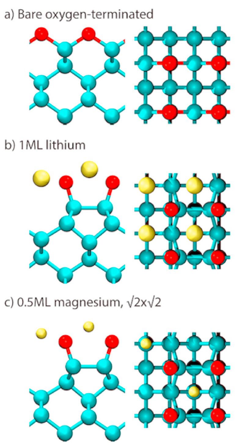
This hydrogenated NEA diamond surface is an excellent candidate for many applications requiring efficient sources of electrons. However, due to the fragility of the H termination, a great deal of effort has been expended, by ourselves and other groups, to find a suitable diamond surface termination that exhibits similar or improved NEA properties to hydrogen-terminated diamond but with greater stability at higher temperatures and with high electron emission currents. Most work on alternative termination species has involved depositing monolayers or sub-monolayers of electropositive metals (M), such as Li, Mg, Na, Ti, Al, and Sc, directly onto the diamond surface. Relatively few metal adsorbates have been studied experimentally to date, but several of those have shown promising emission characteristics. However, although many of these metals may establish a useful NEA surface when adsorbed onto diamond at room temperature, due to weak M�C bonding, at elevated temperatures they often desorb or the surface reconstructs into a non-NEA form. Additionally, many of these metals oxidise easily, so on exposure to air, the M�C bonds break in favour of new M�O bonds, and the NEA surface is again destroyed. One approach to solve these issues is to pre-oxidise the diamond surface before metal deposition. While it may appear counterintuitive to surface terminate with electronegative O, provided a sufficiently electropositive metal is bonded on top of the oxygen layer, the overall M�O�C sandwich can produce a net NEA surface. At Bristol, we have investigated a number of such sandwich structures both experimentally and theoretically, and made a few general observations, which apply to both M�C and M�O�C surface structures. Results suggest that small metal adsorbates (Li+, Na+) are preferable to larger ones because they lie closer to the diamond surface and thus have high adsorption energies with increased temperature stability. Metals with high electropositivity, or which ionise easily to form highly charged ions (Mg2+, Al3+, Ti4+, Sc3+), and which form strong, stable bonds with both C and O, are also good candidates for further investigation. Indeed, we have recently found that scandium-terminated diamond has the highest NEA for a metal adsorbed onto bare diamond measured to date (�1.45 and �1.13 eV on diamond (100) and (111) surfaces, respectively), as well as being thermally stable up to 900 °C. Si and Ge terminations have also been investigated experimentally and theoretically, and look very promising.
|
 Calculated locations of the metal atoms for 3 different diamond surface termination schemes. The side view os on the left, and the plan view on the right. C = blue, O = red, Metal = Yellow. ML = monolayer. |
Diamond with terminating groups that afford robust NEA surfaces would be extremely useful in a wide range of electron-emission applications, which would become significantly more efficient and reliable if the electrons travelling out of the diamond surface had to overcome a much reduced or zero energy barrier. Example applications include:
- Field emission - here a high voltage is used to extract the electrons. This can be used to fabricate cold-cathode devices such as ultra-fast transistors or emissive flat-panel displays.
- Thermionic emission - here a high temperature is used to extract the electrons. This can enable thermionic power generators which produce electricty from heat - e.g. solar radiation.
- Betavoltaic emission - here beta radioactivity produces electrons. This can enable 'nuclear batteries' with lifetimes of many thousands of years.
- Secondary electron emission - here a high-energy primary electron beam generates multiple secondary electrons which are emitted from the diamond surface. Electron amplification like this can be used to fabricate photomultipliers or night-vision goggles.
Related Papers
- K.M. O�Donnell,, T.L. Martin, N.A. Fox and D. Cherns, "The Li-adsorbed C(100)-(1x1):O Diamond Surface", Mater. Res. Soc. Symp. Proc. 1282 (2011)
- K. M. O�Donnell, T. L. Martin, N. A. Fox, and D. Cherns, "Ab initio investigation of lithium on the diamond C(100) surface", Phys. Rev. B 82, (2010) 115303
- Tomas Martin, PhD thesis, University of Bristol July 2011, "Lithium-oxygen termination as a negative electron affinity surface on diamond: a computational and photoemission study".
- M.C. James, P.W. May, A. Croot, N.L. Allan, "A Theoretical Study of Negative Electron Affinity from Aluminium on the Diamond (100) Surface", J. Phys.: Condens. Matter 30 (2018) 235002.
- H. Dominguez-Andrade, A. Croot, G. Wan, J.A. Smith, N.A. Fox, "Characterisation of thermionic emission current with a laser-heated system", Rev. Sci. Instrum. 90 (2019) 045110.
- M.C. James, P.W. May, N.L. Allan, "Ab initio study of negative electron affinity from light metals on the oxygen-terminated diamond (111) surface", J. Phys.: Condens. Matter 31 (2019) 295002.
- H. Dominguez-Andrade, J. Anaya, A. Croot, M. Cattelan, D.J. Twitchen, M. Kuball, N.A. Fox, "Correlating Thermionic Emission with Specific Surface Reconstructions in a <100> Hydrogenated Single-Crystal Diamond", ACS Appl. Mater. Interfaces 12 (2020) 26534.
- M.C. James, F. Fogarty, R. Zulkharnay, N.A. Fox, P.W. May, "A Review of Surface Functionalisation of Diamond for Thermionic Emission Applications", Carbon 171 (2020) 532.
- S. Ullah, G. Wan, C. Kouzios, C. Woodgate, M. Cattelan, N.A. Fox, "Structure and electronic properties of Tin monoxide (SnO) and lithiated SnO terminated diamond (100) and its comparison with lithium oxide terminated diamond", Appl. Surf. Sci. 559 (2021) 149962.
- M.C. James, M. Cattelan, N.A. Fox, R.F. Sila, R.M. Silva, P.W. May, "Experimental Studies of Electron Affinity and Work Function from Aluminium on Oxidised Diamond (100) and (111) Surfaces", Physica Status Solidi B: Basic Solid State Phys. (2021) 2100027.
- Michael C. James, PhD, "Aluminium and Oxygen Termination of Diamond for Thermionic Applications", February 2020.
- Yuet Mun Gary Wan, PhD, "Characterization of Electron Emission From Diamond Surfaces For Energy Conversion Devices", January 2021.
- S. Ullah, N.A. Fox, "Modification of the Surface Structure and Electronic Properties of Diamond (100) with Tin as a Surface Termination: A Density Functional Theory Study", J. Phys. Chem. C 125 (2021) 25165. [doi: 10.1021/acs.jpcc.1c05973].
- R. Zulkharnay, N.L. Allan and P.W. May, "Ab initio study of negative electron affinity on the scandium-terminated diamond (100) surface for electron emission devices", Carbon 196 (2022) 176-185. [doi: 10.1016/j.carbon.2022.04.067].
- F. Fogarty, N.A. Fox, P.W. May, "Experimental Studies of Electron Affinity and Work Function from Titanium on Oxidised Diamond (100) Surfaces", Funct. Diamond 2 (2022) 103-111. [doi: 10.1080/26941112.2022.2122733]
- R. Zulkharnay, P.W. May, "Experimental Evidence for Large Negative Electron Affinity from Scandium-terminated Diamond", J. Mater. Chem. A 11, (2023) 13432-13445. [doi: 10.1039/D2TA09199B]
- R. Zulkharnay, G. Zulpukarova, P.W. May, "Oxygen-terminated diamond: insights into the correlation between surface oxygen configurations and work function values", Appl. Surf. Sci. 658, (2024) 159776. [doi: 10.1016/j.apsusc.2024.159776]
- R. Zulkharnay, N.A. Fox, P.W. May, "Enhanced Electron Emission Performance and Air-Surface Stability in ScO-terminated Diamond for Thermionic Energy Converters", Small 20 (2024) 2405408. [doi: 10.1002/smll.202405408]

