
 Tetrahedral Amorphous Carbon Films
These ta-C films were produced by pulsed laser deposition using graphite targets. See here for more details on film production.
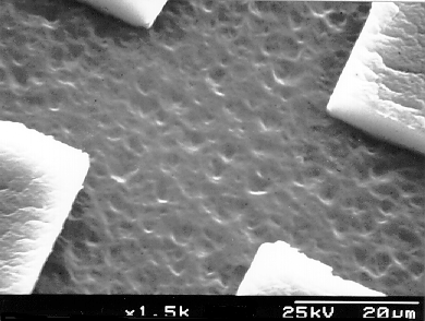 |
An SEM photo of a patterned ta-C film. The film is seen at the corners, and the Si substrate is seen in the centre of the image. The film is around 200 nm thick. |
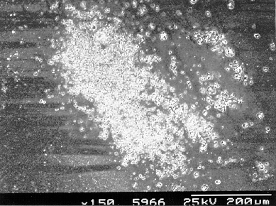 |
An SEM photo of a ta-C film after electron emission testing. The emission site has become roughened, compared to the smooth surface seen before emssion at the edges of the photo. It is believed that the emission process 'burns off' any graphitic component to the films, leaving an enhanced diamondlike nodules. This improves the threshold voltage and stability of the emission. |
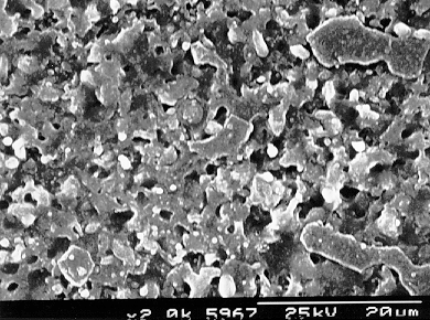 |
A close up SEM shot of the emission site, highlighting the 'diamond' nodules. |