
 Damage Craters seen after Field Emission Testing of Diamond Films
CVD diamond and DLC films are routinely tested for field emission of electrons. After testing, the surface of the films often exhibit morphology changes, from small indents to large craters. The creation and evolution of these craters are discussed in our paper in J. Appl. Phys. (1998).
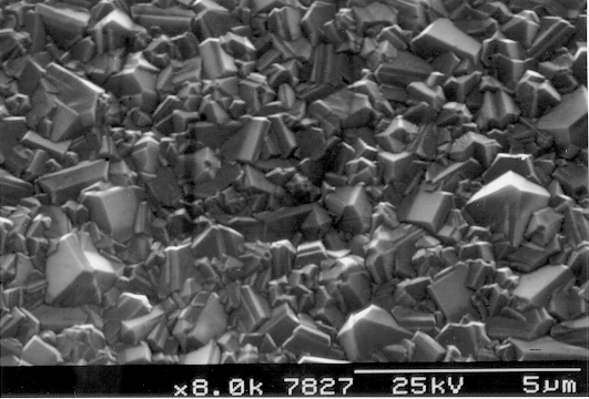 |
Surface of CVD diamond film before Field Emission testing. |
 |
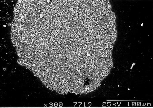
After extracting about 1μA for 30 s, the diamond surface becomes covered in a black graphitic layer. |
 |
After extracting 1μA for 5 mins we see small craters starting to appear. |
 |
After extracting 1μA for 30 mins the craters have deepened to reach the Si substrate. |
 |
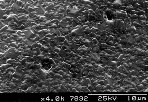
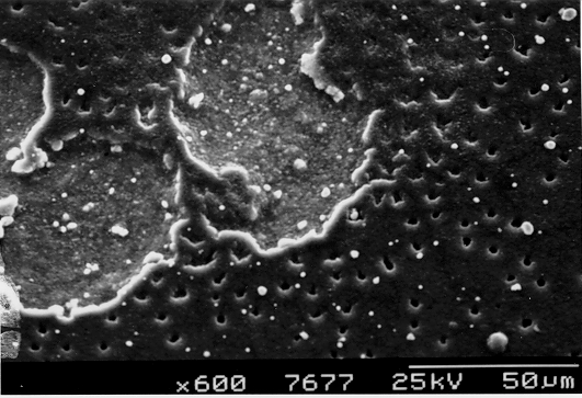
After extracting 10μA for 10 mins the crater density has increased. We've christened this the 'Ryvita effect' since the surface looks like a piece of Swedish crispbread! |
 |
After extracting 10μA for 30 mins the craters density has increased further so that some craters have started to join together and the film is delaminating or being burnt away in large sections |
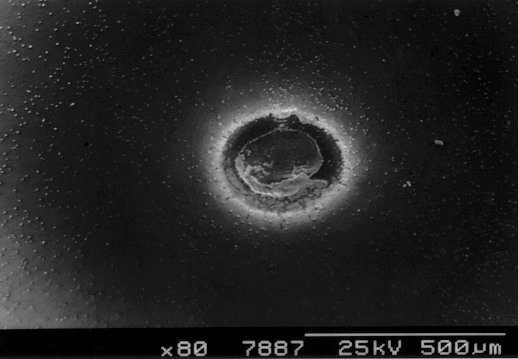 |
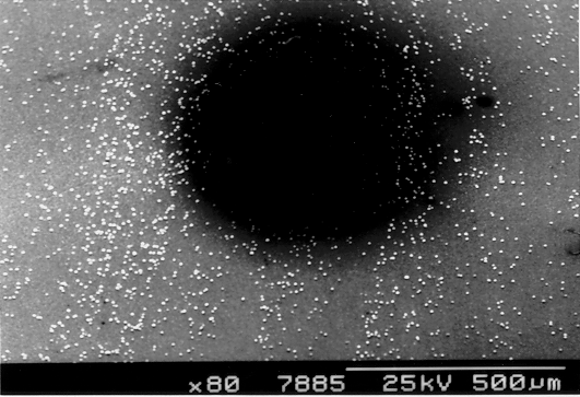
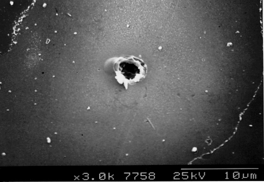
After extracting 100μA for 30 mins we see one large crater with extensive damage to the surrounding area. |
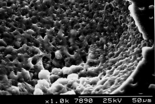 |
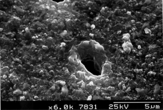
A close up of the central area of the above crater showing the extensive melting and recrystallisation of the Si substrate. |
 |
A 'graphitic' DLC film after FE testing, showing a uniform pitting of the surface. |
 |
A 'medium' DLC film after FE testing, showing the Ryvita effect. |
 |
A 'diamondlike' DLC film after FE testing, showing a single deep, large crater. |
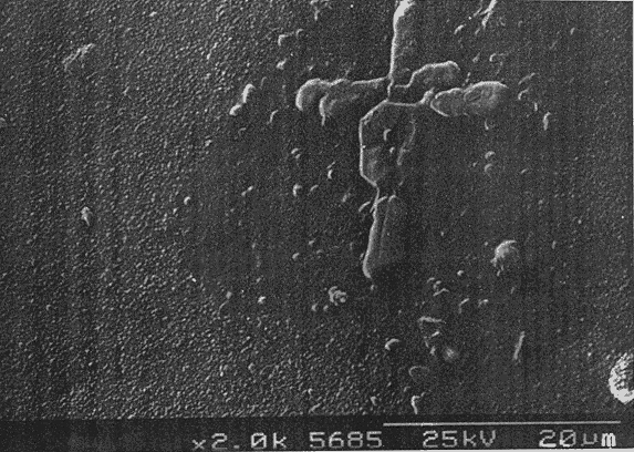 |
A CVD diamond film grown on n-type Si ater FE testing. Note the straight line blisters. |
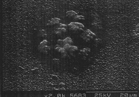 |
A CVD diamond film grown on p-type Si ater FE testing. Note the cauliflower shaped blisters. |